
Nanotech breakthrough: get ready for graphene. The exciting one-atom thick super material can now be produced in ample quantities and high quality.
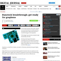
Rapid improvements in nanotechnology are now expected. Technology improvements are about to get dramatically ultra-fast. Exciting sustaining and disruptive innovations are on the way for just about every digital appliance, from touchscreen tablet computing to solar cells, according to a Science Daily report. Graphene is a new form of carbon, one atom in thickness, extremely strong and highly conducive. High performance can be achieved with graphene transistors that can operate at much faster speeds and in higher heat conditions compared to current silicon chip technology. My Site. Latest science discovery. National Science Foundation (NSF) Discoveries - The Nanotechnology of Sundew and English Ivy.
DiscoveryThe Nanotechnology of Sundew and English Ivy Researchers are studying the adhesive properties of sundew plants and the nanoparticles in English ivy for innovative medical applications October 17, 2011 Fifteen small sundew plants perch on a window sill, collecting sunlight and eating meat in the lab of Mingjun Zhang on the University of Tennessee's Knoxville campus.
Sundew plants are carnivores, consuming insects by capturing them with small adhesive balls on the ends of their tentacles. The tentacles and their adhesive properties may be nature's design for catching insects, but Zhang's research team hopes that one day this same adhesive can help attach your grandmother's replacement hip or your artificial knee without fear that your bodies will reject it. Finding organic biomaterials In medical replacement operations, "you need something cells can recognize and attach to," Lenaghan said. Medical uses The sundew's adhesive has "Spiderman" qualities.
Other uses Total Grants $575,259. Nanotechnology. Oak Ridge National Laboratory - ORNL experiments prove nanoscale metallic conductivity in ferroelectrics. ORNL study pegs fuel economy costs of common practices OAK RIDGE, Tenn., April 9, 2014 – People who pack their cars and drive like Clark Griswold in National Lampoon’s “Vacation” pay a steep penalty when it comes to fuel economy, according to a report by the Department of Energy’s Oak Ridge National Laboratory.
Vertimass licenses ORNL biofuel-to-hydrocarbon conversion technology OAK RIDGE, Tenn., March 6, 2014 — Vertimass LLC, a California-based start-up company, has licensed an Oak Ridge National Laboratory technology that directly converts ethanol into a hydrocarbon blend-stock for use in transportation fuels. Icenhour to lead ORNL's Nuclear Science and Engineering Directorate OAK RIDGE, Tenn., Feb. 27, 2014 -- Alan Icenhour has been named associate laboratory director for Nuclear Science and Engineering at the Department of Energy's Oak Ridge National Laboratory. ORNL establishes Liane B.
Russell Distinguished Early Career Fellowship OAK RIDGE, Tenn. A Nanotube Space Elevator. The chemical element carbon is one the most abundant elements in the universe.

The structure of carbon lends itself to make millions of different compounds; it has four valence electrons, allowing it to bond with up to four other atoms at a time. In one form of carbon—graphite—each carbon atom is bonded to three other carbon atoms in a plane of hexagonal rings; the bonds within the plane are extremely strong, even stronger than in diamond. Starting in the late 20th century, a great deal of research has been focused on fullerenes, a form of carbon that is similar in structure to the plane of hexagonal rings in a single layer of graphite, but formed into shapes such as hollow spheres (buckyballs) and cylinders (nanotubes). In particular, carbon nanotubes, which are essentially tiny tubes of carbon with a diameter of just about a nanometer (a billionth of a meter), have exceptional properties that seem to give them unlimited potential for use.
Nanotech breakthrough: get ready for graphene. IIT Researchers Prove Homeopathy is Based on Nanotechnology. IIT Researchers Prove Homeopathy is Based on Nanotechnology IIT scientists have said the homeopathic medicines work on the principle of nanotechnology.
Homeopathic pills containing metals such as gold, copper and iron retain their potency even when diluted to a nanometre or one-billionth of a metre, states the IIT-Bombay research published in the latest issue of ‘Homeopathy’, a peer-reviewed journal. IIT-B’s chemical engineering department bought homeopathic pills from neighbourhood shops, prepared highly diluted solutions and checked these under powerful electron microscopes to find nanoparticles of the original metal. ”Certain highly diluted homeopathic remedies made from metals still contain measurable amounts of the starting material, even at extreme dilutions of 1 part in 10 raised to 400 parts (200C),” said Dr Jayesh Bellare from the scientific team.
“Homeopathy has been a conundrum for modern medicine. Homeopathic Medicine is Nanopharmacology. Dana Ullman invites us to think of homeopathy as medicine at ultra-small doses, or nanopharmacology, which avoids the often debilitating side effects of conventional pharmacology.
If you wish to see the complete document with references, please consider becoming a member or friend of ISIS. Full details here Nanotechnology. Electromagnetic spectrum. The electromagnetic spectrum is the range of all possible frequencies of electromagnetic radiation.[4] The "electromagnetic spectrum" of an object has a different meaning, and is instead the characteristic distribution of electromagnetic radiation emitted or absorbed by that particular object.
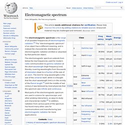
Most parts of the electromagnetic spectrum are used in science for spectroscopic and other probing interactions, as ways to study and characterize matter.[6] In addition, radiation from various parts of the spectrum has found many other uses for communications and manufacturing (see electromagnetic radiation for more applications). History of electromagnetic spectrum discovery The first discovery of electromagnetic radiation other than visible light came in 1800, when William Herschel discovered infrared radiation.[7] He was studying the temperature of different colors by moving a thermometer through light split by a prism. He noticed that the highest temperature was beyond red. Where: Title, Abstract Query Results. Nanometre. The nanometre (International spelling as used by the International Bureau of Weights and Measures; SI symbol: nm) or nanometer (American spelling) is a unit of length in the metric system, equal to one billionth of a metre.
The name combines the SI prefix nano- (from the Ancient Greek νάνος, nanos, "dwarf") with the parent unit name metre (from Greek μέτρον, metrοn, "unit of measurement"). It can be written in scientific notation as 1×10⁻⁹ m, in engineering notation as 1 E−9 m, and is simply 1 / 1,000,000,000 m. One nanometre equals ten angstroms. Use[edit] The nanometre is often used to express dimensions on an atomic scale: the diameter of a helium atom, for example, is about 0.1 nm, and that of a ribosome is about 20 nm. History[edit] The nanometre was formerly known as the millimicrometre – or, more commonly, the millimicron for short – since it is 1/1000 of a micron (micrometre), and was often denoted by the symbol mµ or (more rarely) µµ.[2][3][4] In 1960, the U.S.
References[edit] Atomic force microscopy. An atomic force microscope on the left with controlling computer on the right.
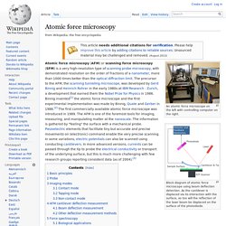
Block diagram of atomic force microscope using beam deflection detection. As the cantilever is displaced via its interaction with the surface, so too will the reflection of the laser beam be displaced on the surface of the photodiode. Atomic force microscopy (AFM) or scanning force microscopy (SFM) is a very high-resolution type of scanning probe microscopy, with demonstrated resolution on the order of fractions of a nanometer, more than 1000 times better than the optical diffraction limit. The precursor to the AFM, the scanning tunneling microscope, was developed by Gerd Binnig and Heinrich Rohrer in the early 1980s at IBM Research - Zurich, a development that earned them the Nobel Prize for Physics in 1986. Basic principles[edit]