
Voxel8 Launches World’s First 3D Electronics Printer at CES; Partners with Autodesk. BOSTON--(BUSINESS WIRE)--Voxel8, creator of the world’s first multi-material 3D electronics printer and backed by Braemar Energy Ventures, today announced pre-order availability of its initial product – the Voxel8 Developer’s Kit – on its website, www.voxel8.co.
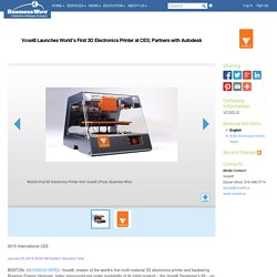
Voxel8 also announced its partnership with Autodesk to develop a new design tool called Project Wire for creating 3D electronic devices printed on Voxel8’s platform. Together, Voxel8 and Autodesk are enabling designers and engineers to create three-dimensional parts with embedded circuitry for the first time. “Voxel8 is leveraging over a decade of research, which has led to 17 patents (10 issued) on functional materials, printheads, and other processes for 3D printing, from my lab” The Voxel8 Developer’s Kit will include the desktop 3D electronics printer, conductive ink cartridges, PLA filament, modeling software and software support. Semiconductor Research Corporation - SRC. RESEARCH TRIANGLE PARK, N.C.

(May 7, 2014) – University of California, Berkeley researchers sponsored by Semiconductor Research Corporation (SRC), the world’s leading university-research consortium for semiconductors and related technologies, are pursuing a novel approach to 3D device integration that promises to lead to advanced mobile devices and wearable electronics featuring increased functionality in more low-profile packages. The research focuses on integrating extra layers of transistors on a vertically integrated 3D monolithic chip using printing of semiconductor “inks” as compared to the current method of chip-stacking through 3D interconnect solutions.
The new process technology could help semiconductor manufacturers develop smaller and more versatile components that are less expensive and higher performing by enabling cost-effective integration of additional capabilities such as processing, memory, sensing and display. Rabbit Proto & 3D Printed Circuit Projects. IBM's 3D Printer to Revolutionize Chip Prototyping. Another Sub-mm 3D Printed Model. Microscale printing of a spaceship on world's fastest 3D printer. Feb.9, 2013 The video below shows a real-time recording of the 3D micro printing process by two-photon polymerization.
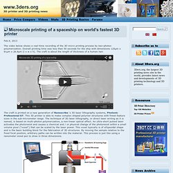
Overall printing time was less than 50 seconds for the ship with dimensions 125µm x 81µm x 26.8µm (l x w x h). The craft is about the length of thickness of a human hair. The craft is printed on a new generation of Nanoscribe´s 3D laser lithography systems, Photonic Professional GT. This 3D printer is able to make complex shaped polymer structures with finest feature sizes in the sub-micrometer range. Researchers start with the CAD model of the ship, based a Hellcat spaceship from Wing Commander Saga and then use Photonic Professional GT 3D printer to print a polymer model on the microscale. Key features: A Simple, Low-Cost Conductive Composite Material for 3D Printing of Electronic Sensors. 3D printing technology can produce complex objects directly from computer aided digital designs.

The technology has traditionally been used by large companies to produce fit and form concept prototypes (‘rapid prototyping’) before production. In recent years however there has been a move to adopt the technology as full-scale manufacturing solution. The advent of low-cost, desktop 3D printers such as the RepRap and Fab@Home has meant a wider user base are now able to have access to desktop manufacturing platforms enabling them to produce highly customised products for personal use and sale. This uptake in usage has been coupled with a demand for printing technology and materials able to print functional elements such as electronic sensors.
Figures Citation: Leigh SJ, Bradley RJ, Purssell CP, Billson DR, Hutchins DA (2012) A Simple, Low-Cost Conductive Composite Material for 3D Printing of Electronic Sensors. Copyright: © 2012 Leigh et al. Introduction Results and Discussion Figure 1.
Conductive Abs @Repraper. Silicon micro/nano structures. Jun.28, 2012 Researchers at KTH Microsystem Technology have demonstrated a new technology for printing 3D silicon micro- and nanostructures.
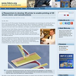
Silicon is the material used to manufacture integrated circuits and other micro-sized electronic devices. Production of silicon micro- and nanosensors with current technologies requires a full-scale clean-room laboratory and highly complicated fabrication schemes. This team led by Frank Niklaus, Associate Professor at KTH Microsystem Technology received a grant of EUR 1.5 million (about SEK 15 million) from the European Research Council for their research on new manufacturing paradigms for micro- and nanosystems.
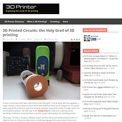
Printed circuits. Printed circuits have often been referred to as the “holy grail” in 3D printing.
With this capability, a single machine could produce an entire electrical/mechanical device out of a digital file. This would vastly expand the productive repertoire of these machines, beyond the variety of shapes built from non-conductive plastics. The folks over at the RepRap Blog have had some inspiring success extruding a conductive metal, but there is another project attempting to do something similar. The project, 3D-PCB, is actually a software project aimed at the proliferating low-end printers. It takes the form of a library for OpenSCAD, a modeling language which allows object forms to be created using code instead of more traditional design techniques. The current capabilities are detailed in an instructable, and contains instructions for building a simple circuit, how to wrap it all together, and an example application: an LED flashlight.
Here’s the description of that Instructable: