
How to Make a Custom PCB - Circuit Basics. Breadboards are great for prototyping circuits, but they aren’t so good for actually using the thing you’re building.
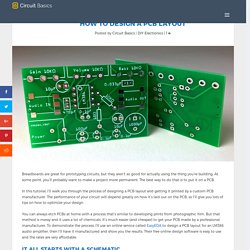
At some point, you’ll probably want to make a project more permanent. The best way to do that is to put it on a PCB. In this tutorial, I’ll walk you through the process of designing a PCB layout and getting it printed by a custom PCB manufacturer. The performance of your circuit will depend greatly on how it’s laid out on the PCB, so I’ll give you lots of tips on how to optimize your design. You can always etch PCBs at home with a process that’s similar to developing prints from photographic film. It All Starts With a Schematic Before you start designing your PCB, it’s a good idea to make a schematic of your circuit.
Start by logging in to EasyEDA, and create a new project: Once you’re on the Start page, click on the “new Schematic” tab: Now you’ll see a blank canvas where you can draw the schematic: The CircuitCalculator.com Blog » PCB Trace Width Calculator. This Javascript web calculator calculates the trace width for printed circuit boards based on a curve fit to IPC-2221 (formerly IPC-D-275).
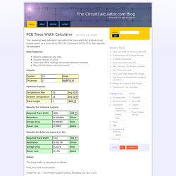
Also see the via calculator. New features: Results update as you type Several choices of units Units and other settings are saved between sessions Blog format allows user comments Inputs: Optional Inputs: Results for Internal Layers: Results for External Layers in Air: Notes: The trace width is calculated as follows: First, the Area is calculated: Area[mils^2] = (Current[Amps]/(k*(Temp_Rise[deg. Then, the Width is calculated: Width[mils] = Area[mils^2]/(Thickness[oz]*1.378[mils/oz]) For IPC-2221 internal layers: k = 0.024, b = 0.44, c = 0.725 For IPC-2221 external layers: k = 0.048, b = 0.44, c = 0.725 where k, b, and c are constants resulting from curve fitting to the IPC-2221 curves For geometry diagrams, click on the pictures below.
For frequently asked questions, see the comments. EasyEDA - Online PCB design & circuit simulator. Editing PCB Objects. The properties of an object can be edited in a dialog, or in the PCB Inspector panel.
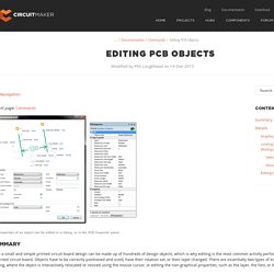
Summary Even a small and simple printed circuit board design can be made up of hundreds of design objects, which is why editing is the most common activity performed while designing a printed circuit board. Objects have to be correctly positioned and sized, have their rotation set, or their layer changed. There are essentially two types of editing: graphical editing, where the object is interactively relocated or resized using the mouse cursor; or editing the non-graphical properties, such as the layer, the font, or the line width.
Details An object can have it's non-graphical properties edited in the following ways: Double mouse-click on the object to open the properties dialog. Graphical Editing Graphical properties, such as the size or location of the object, are generally edited interactively. Make a proper PCB exposer out of a cheap UV nail curing lamp. What do PCB production and fake fingernails have in common?
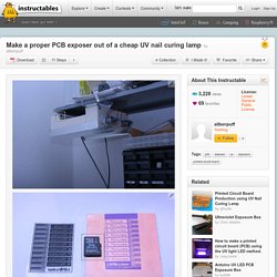
They both use UV light sources of high intensity and, as luck would have it, those light sources have exactly the same wavelength. Only the ones for PCB production are usually quite costly and the ones for fake fingernails are a bit more competitively priced. This instructable is about how to use such a device to build a low cost light source, suitable for exposing the various UV sensitive materials encountered in printed circuit board production, like dry film photoresist and UV curable soldermask.
As well as being very low cost (around $20 for all required materials), this build addresses a few issues I've seen on other devices on the intertubes: Collimation: To simply expose a board with fairly coarse features, you wouldn't need to do any of this. So, while being very low cost, this build will enable you to achieve results that match, or (in some cases) even surpass those of devices that are up to 10 times more expensive. Designing the Wristband PCB… using DesignSpark and iTead Studio.
These days I use DesignSpark PCB for designing my PCBs.
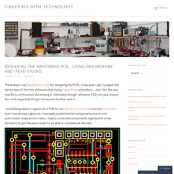
A few years ago, I judged it to be the best of the free software after trying Eagle, Kicad and others – and I like the way that RS is continuously developing it. Ultimately though, whatever CAD tool you choose, the most important thing is to become familiar with it. I used DesignSpark to generate a PCB for my vibrating wristband from the schematic that I had already captured.