
Getting Started With PCB. Table of Contents This document is a manual for PCB, the interactive printed circuit board layout system. 1 Introduction PCB includes a stand-alone program (called pcb) which allows users to create, edit, and process layouts for printed circuit boards, as well as a library of footprint definitions for commonly needed elements.
While originally written for the Atari, and later rewritten for Unix-like environments, it has been ported to other operating systems, such as Linux, MacOS/X, and Windows. While PCB can be used on its own, by adding elements and traces manually, it works best in conjunction with a schematic editor such as gschem from the gEDA project, as gschem will create a netlist, make sure all the elements are correct, etc.
Lf355, Applications: Using gEDA. Introduction Why another article to talk about EDA, Electronic Design Automation?
Because there is more than one way to do it and this one is free. One of its best particularity is the fact that we have a set of tools, some graphical ones but mostly command line based. With this article, I will just show how to make a PCB (Printed Circuit Board) from the beginning. What is gEDA? gEDA PCB Footprint Creation Utility. This utility automatically creates the contents of common types of footprint files for the gEDA PCB layout tool.
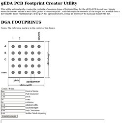
Simply enter the correct values in each field, press "Create Footprint", and then copy the contents of the output text window into a file with the name "partname.fp". If the part has special features, it may be necessary to manually modify the file. Notes: The reference mark is in the center of the device. Notes: gEDA Project's Homepage. gEDA Resources - Evil Mad Scientist Wiki. Geda:gsch2pcb_tutorial [gEDA Project Wiki] Translations of this page are also available in the following languages: Русский.
![geda:gsch2pcb_tutorial [gEDA Project Wiki]](http://cdn.pearltrees.com/s/pic/th/geda-gsch2pcb-tutorial-project-90361744)
This is a tutorial on the process of using gsch2pcb as an interface between gschem and PCB. It assumes the gEDA, PCB and gsch2pcb packages are already installed and ready to use. Starting with gEDA 20030901, gsch2pcb is packaged with gEDA and doesn't need to be separately installed. This tutorial is functional and intended to generate results as quickly as possible. It is not a complete reference on gschem or PCB, but it does show with a simple example design all the steps one might need to take. The goal is to use gsch2pcb as the bridge between gschem and PCB so that the schematics can always be in sync with the PCB layout because all element additions or deletions in the layout will automatically be driven by changes in the schematics.
See the release notes for the history of this tutorial. Terminology. gEDA tutorial - Hobby Electronics. This is a short tutorial on using gEDA for round-trip engineering.
Contents Creating schematics Start gschem with: gschem my-schematic.sch Press [I] to insert a part. Pcb. Pcb This document is a manual for Pcb, the open source, interactive printed circuit board layout system.
Copying Copyright © 1994,1995,1996,1997 Thomas Nau Copyright © 1998,1999,2000,2001,2002 harry eaton This program is free software; you may redistribute it and/or modify it under the terms of the GNU General Public License as published by the Free Software Foundation; either version 2 of the License, or (at your option) any later version. Getting Started With PCB. PCB design & fabrication (Procedure) : FAB laboratory : Mechanical Engineering : COE PUNE Virtual Lab. Capolight Electronics Projects. How to use cad.py.
Repairable Machines. This tutorial uses our modified CAD.PY version 5/5/11 .
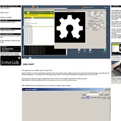
We use CAD.PY to convert a 2D-bitmap to machine code. This machine code is called G-code, and is sent to the machine later using a separate piece of software, ReplicatorG. The image on top of this page shows CAD.PY on the right and ReplicatorG, displaying the G-code, on the left. In this tutorial we will open a black & white bitmap, set the correct size and depth, generate the G-code and save it. Alternatively, you can get started using the calibration test files on our DOWNLOADS page.
After installing Python, and opening cad.py, you should see a similar screen as below: Click on 'INPUT' and select a bitmap. Land_patterns_20070818.pdf. How to make PCBs with the Modela (cad.py) Starting out The modela is a nice little milling machine that cranks out most of the circuits you will need for HTMAA.
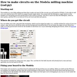
To be able to mill on it, you need to have FR1 which is a paper based copper plate. You cannot mill the fiberglass copper plates on the modela as it will break your bit and the dust it will create is irritant. The FR1 is more tan than the fiberglass, which is more green, and the FR1 is in stock in 016 in 2x3 inch and 4x6 inch pieces. Where do you get the circuit You can either use a b/w .png with 500 resolution, which can be output by eagle, or a .cad file written for cad.py. Printed circuit board milling. Milled Printed Circuit Board Printed circuit board milling (also: isolation milling) is the process of removing areas of copper from a sheet of printed circuit board material to recreate the pads, signal traces and structures according to patterns from a digital circuit board plan known as a layout file.

Similar to the more common and well known chemical PCB etch process, the PCB milling process is subtractive: material is removed to create the electrical isolation and ground planes required. However, unlike the chemical etch process, PCB milling is typically a non-chemical process and as such it can be completed in a typical office or lab environment without exposure to hazardous chemicals. High quality circuit boards can be produced using either process. Advantages[edit] Gschem warmup. You need to become familiar with doing a few things in gschem, so just run gschem and start playing around: You get an initial blank page with a menus and a toolbar at the top.
As you select operations from the menus, notice that there are usually keyboard shortcuts which can alternatively be used to access the menu functions. When drawing a schematic, It's a good idea to always start by setting some schematic boundaries to draw within, so we will do this by adding a titleblock. I find that using a B sized titleblock lets my schematics print at a nice size on letter sized paper: Bring up the Select Component window by selecting from the menu Add->Component or hit keyboard shortcut i.
Creating Your Own Symbols in gschem. Before writing another tutorial on SPICE, I thought of spending some time on creating symbols. This will be necessary because we will be looking at op-amp circuits next. There are op-amps in the gschem library but there are incompatibilities between those and the model files which the manufacturers provide. While trying to figure out how to create symbols, I found an excellent 3 part tutorial on this. I will take you through the creation of an op-amp symbol in this tutorial but I still feel this video will do better than that. Geda:gschem_symbol_creation [gEDA Project Wiki] Translations of this guide are also available in the following languages: Русский Overview This document describes the creation of component symbols, including style conventions, and hints/tips and things to look out for when drawing symbols for the gEDA/gaf system.
Component Symbol Creation. Software and Hardware Index. Screen shot KCam Router/Mill software is designed to run low cost hobby CNC equipment. Program your paths using the built in Gcode editor, or import DXF, NC, and PLT files. Create signs and plates using your CAD software and import your work into KCam. Dual cutting depth allows for holes and outlines to be punched out after routing. No more drilling holes for switches or cutting plates to size before engraving. Engrave signs, make name tags, drill printed circuit boards, mill parts, plasma cuts, plot pictures onto paper... Here are a few of the key features:
GerberGrab- Utilities for reverse engineering and verifying assembly data. Gerber to HPGL converter. Software of the finest. PCB Milling. PCB Milling Release status: Concept. Gsch2pcb tutorial. gEDA PCB Footprint Creation Utility. Geda:gschem_ug:config [gEDA Project Wiki] Geda:gsch2pcb_tutorial [gEDA Project Wiki] gEDA Project's Homepage. Circuit Design on Your Linux Box Using gEDA. PCB Home Page.