
Making PCB - Kavionic. Dual sided PCB with solder mask, tinning, vias, and plated through holes.
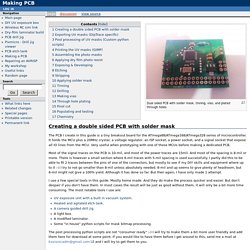
Creating a double sided PCB with solder mask The PCB I create in this guide is a tiny breakout board for the ATmega88/ATmega168/ATmega328 series of microcontroller. It holds the MCU plus a 20MHz crystal, a voltage regulator, an ISP socket, a power socket, and a signal socket that expose all IO lines from the MCU. Very useful when prototyping with one of those MCUs before making a dedicated PCB.
Most of the signal traces on the PCB is 10-mil, and most of the power traces are 15mil. I use a few special tools in this guide. The post processing python scripts are not "consumer ready" :-) I will try to make them a bit more user friendly and add them here for download at some point. Please try anything you see me do at home. Exporting UV masks (DipTrace specific) This section is very specific to DipTrace which is my schematics capture and PCB layout package of choice.
As you can see, I have included the "Assy" layer here. Killer PCBs. After experimenting with home PCB fabbing for a while, I've finally worked out a process that produces reasonably consistent results that actually look pretty good.
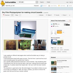
I spent lots of time trying to use the toner transfer method with varying degrees of success (OK, varying degrees of failure might be more accurate). I also tried Philmore/Datak negative photo resist spray with consistently horrible results (the stuff eventually melted the spray nozzle that came with it and leaked all over the place). Not Green & not recommended. Now I could have purchased presensitized boards and saved a lot of trouble, but I find the material to be too costly for the volume of boards I'm producing. I eventually tried dry film photo resist and I won't be going back! If you haven't tried the toner transfer method, do so. Thus far, I've used three types of dry film resist, all of which performed well:--MG Chemicals 416DFR Dry Film Resist About $20.00 for 12" by 5 feet at Frys, Altex and online.
Dry Film Photopolymer for making circuit boards - All. I was reading on different web pages what could be the better way on doing a printed circuit.
EAGLE Library - New and improved EAGLE part libraries - CadSoft. Make Your Own D*mn Board – Part 1: Layout. There are many tools for creating printed circuit boards, from the open source KiCAD to various online services.
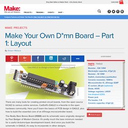
CadSoft’s EAGLE is a favorite in the open hardware community. Here you’ll learn the basics of PCB design in EAGLE, plus how to build the essential core of an ATmega microcontroller board. The Really Bare Bones Board (RBBB) and its schematic were originally designed by Paul Badger of Modern Device. It’s pretty much the bare minimum needed for a useful Arduino-type development board. And once you build the schematic in EAGLE, it’s easy to incorporate in other designs. NOTE: The part list, to right, gives the bill of materials for a single RBBB, but you don’t really need the components on-hand to follow along with the design tutorial below. Jean-Claude Wippler of JeeLabs used the RBBB as a basis design for JeeNode, which has rearranged headers and an SPI radio port for wireless use. Using EAGLE EAGLE is a collection of programs, each serving one part of the design process. 1. 1.1.
How to Install and Setup EAGLE. Favorited Favorite 9 Introduction Printed circuit boards (PCBs) are the backbone of every electronic gizmo out there.
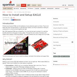
They’re not flashy like those microprocessors, or abundant like resistors, but they’re essential to making all components in a circuit connect together just right. We LOVE designing PCBs here at SparkFun. It’s a love that we want to spread. This first tutorial goes over how to install the software, and tailor-fit its interface and support files. Using EAGLE: Schematic. Favorited Favorite 6 Introduction PCB design in EAGLE is a two-step process.
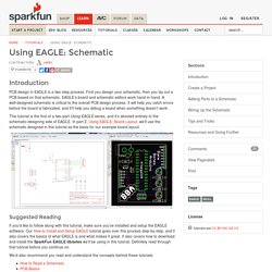
First you design your schematic, then you lay out a PCB based on that schematic. EAGLE’s board and schematic editors work hand-in-hand. A well-designed schematic is critical to the overall PCB design process. This tutorial is the first of a two-part Using EAGLE series, and it’s devoted entirely to the schematic-designing side of EAGLE. Suggested Reading If you’d like to follow along with this tutorial, make sure you’ve installed and setup the EAGLE software. We’d also recommend you read and understand the concepts behind these tutorials:
Using EAGLE: Board Layout. Favorited Favorite 8 Previously on Using EAGLE EAGLE’s board designer is where a good portion of the magic happens.
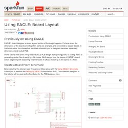
It’s here where the dimensions of the board come together, parts are arranged, and connected by copper traces. In the board editor, the conceptual, idealized schematic you’ve designed becomes a precisely dimensioned and routed PCB. In this tutorial we’ll cover every step in EAGLE PCB design: from placing parts, to routing them, to generating gerber files to send to a fab house. Create a Board From Schematic Before starting this tutorial, read through and follow along with the Using EAGLE: Schematic tutorial (not to mention the Setting Up EAGLE tutorial before that). The schematic from previous tutorial, complete with an ATmega328P, barrel jack connector, LEDs, resistors, capacitors, and connectors.
To switch from the schematic editor to the related board, simply click the Generate/Switch to Board command – Dry Film Photopolymer for making circuit boards.