
Design and Simulation of Phased Arrays For RadarAerospace Applications. By Gent Paparisto, AWR Group, NI Phased array antenna systems, which use sets of two or more antennas, offer improved performance over single antennas and are well-known for their usefulness in radar and aerospace applications.

Phased arrays are seeing increased use in automotive, satellite, public safety, and advanced wireless communications systems. Communication system design software, such as NI AWR Design Environment/Visual System Simulator (VSS), supports the design and analysis of phased arrays, as well as their implementation in a system of antenna elements, power divider/combiners, phase shifters, and other typical components. This article examines how software can be used to simulate both small and large phased arrays in typical configurations.
Design software for complex communication systems enables engineers to examine system architectures, and to formulate suitable specifications for each of the underlying components. 5G Heats Up Base Stations. Before 5G can be deployed commercially on a large scale, engineers have to solve some stubborn problems—including how to make a hot technology a whole lot cooler. 5G-capable modem chipsets are already on the market from Qualcomm, Samsung, Huawei, MediaTek, Intel and Apple, with some 5G service (LTE-Advanced/LTE-Advanced Pro) available in the U.S.
But still mostly missing from the 5G equation are base stations powerful enough to shape and direct an individual RF connection to every subscriber within range, while performing feats of electromagnetic geometry to maintain that connection. A base station in the wireless world is a device that connects other wireless devices to a central hub. RF Components & Test Equipment - everything RF. Mathworks, SiSoft Announce First Products Following Acquisition. The Growing Challenge Of Thermal Guard-Banding. STATS ChipPAC - Integrated Passive Devices (IPD) Enabling IPD Technology STATS ChipPAC’s IPD technology is a key enabler featuring silicon-based passive integration of RLC components.
IPDs are a cost effective way to reduce footprint, reduce interconnection complexity, improve component tolerance, yield and reliability. By integrating and fabricating passive devices at the silicon wafer level, STATS ChipPAC is able to fabricate IPDs which are significantly smaller, thinner and with higher performance than standard passive devices. To achieve superior IPD performance, STATS ChipPAC employs a copper metallization process capable of depositing 8 microns or more of copper on a silicon wafer. This results in higher Q components that reduce loss in the RF signal transmission path, thereby increasing battery performance of the wireless system and improving reception. IPD Component Library A Comprehensive RF Solution STATS ChipPAC provides the highest level integration of wireless systems. Features Applications. IPD Process Technology – High-Q™ Integrated Passive Device. Download Agreement If you agree to this Agreement on behalf of a company, you represent and warrant that you have authority to bind such company to this Agreement, and your agreement to these terms will be regarded as the agreement of such company.

Integrated passive devices. Integrated Passive Devices (IPD's) "or Integrated Passive Components (IPC's)" are attracting an increasing interest due to constant needs of handheld wireless devices to further decrease in size and cost and increase in functionality.
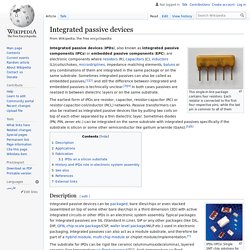
IPD technology offers the ideal trade-off for System in Package (SiP) integration credits to the capability to grind the wafers below 100µm thickness and the flavor of packaging options (micro-bumping, wire bonding, copper pads) and delivery mode options (wafers delivery, tape & reel). In addition, some IPD suppliers offer full design kit support so that System in Package module makers are able to design their own IPD fulfilling their specific and custom requirements.
Integrated Passive Device versus Discrete Surface Mount Devices (SMD) Example of RF IPD balun on Glass Substrate. The 25 Best Classical Music Tracks of 2018. IWPC: The International Wireless Industry Consortium. Embedded-computing. Customers today expect smart products to be portable, compact, aesthetically-pleasing – and able to be connected anywhere and anytime.

That is true for all products nowadays, but especially for consumer products where users expect a sleek look and feel without sacrificing any of the connectivity and performance they expect. Putting a check mark next to that entire wish list is challenging for product engineers, though, because of the inherent tension between a small, aesthetically-pleasing product and robust connectivity. It takes a very careful balance between an antenna’s size, design, and performance to meet customers’ needs while also matching their stylistic preferences for the products’ overall design. As a rule of thumb, the larger the antenna is, the better its wireless range will be – but with that better performance comes challenges about how to make it work for the product you are designing. Antenna Technologies for the Future. Traditional antenna technology has hit its limits in many demanding commercial and aerospace markets such as 5G, SATCOM, IoT and radar.

But there are many companies developing new approaches and materials that could drastically improve antenna performance and enable new applications that were not previously envisioned because of these limitations. In this article, Microwave Journal looks at a sampling of these technologies that have come to our attention in the last couple of years. 3D Printed Antennas Recent advances in 3D printing or additive manufacturing have enabled complex RF structures to be realized. The characterization of the materials used in 3D printing processes has been shown to be critical in designing and accurately predicting the performance of these structures. A NIST Traceable PCB Kit for Evaluating the Accuracy of De-Embedding Algorithms and Corresponding Metrics. Jose Moreira (Senior Staff Engineer, Advantest)Heidi Barnes (Senior Application Engineer, Keysight Technologies)Eric Bogatin (Dean, Teledyne LeCroy Signal Integrity Academy, Teledyne LeCroy)Mikheil Tsiklauri (Research Associate Professor, Missouri University of Science and Technology)Ching-Chao Huang (President, Ataitec)Jim Nadolny (Engineering Manager, Samtec)Jason Ellison (Signal Integrity Engineer, The Siemon Company)Se-Jung Moon (Senior Hardware Engineer, Intel)Volker Herrmann (RF & Microwave Senior Application Engineer, Rohde & Schwarz) Location: Ballroom G Track: 13.

Applying Test and Measurement Methodology. A NIST Traceable PCB Kit for Evaluating the Accuracy of De-Embedding Algorithms and Corresponding Metrics. JiangLong. Dr. Mühlhaus Consulting & Software GmbH » Microwave Office: Antenna matching network efficiency. In part one of this application note we looked at basic design concepts and simulation methods for “printed” PCB antennas.

In part two we investigated co-simulation of antenna and SMD matching components. Now in this third part, we will look in more detail at design and simulation of antenna matching networks, and the loss in antenna matching networks. Calculate the insertion loss of antenna matching networks correctlyOptimize power delivered to the antenna, instead of just minimizing reflected powerAutomated synthesis of antenna matching network This appnote was inspired by Optenni Lab, a powerful matching synthesis software that implements this optimization strategy. Optimize radiated power, not just minimize reflected Only for ideal lossless components, minimum reflection from the antenna ensures maximum radiated power. To reach our goal of optimizing the radiated power, we need to consider the loss introduced by the matching network. Untitled. By Barry Manz for Mouser Electronics Five years from now, the wireless industry as we know it today may be almost completely transformed.

Cellular networks that have always relied mostly on “macro” base stations will be supplemented with hundreds of thousands of “small cells.” 5G Olympic Whitepaper. Spyy005. Verizon plans 5G trial service in 11 cities this year. Lab tests of pre-standard 5G wireless with multi-gigabit speeds are evolving into trial services that users can actually enjoy in the real world – though not necessarily while walking around with a smartphone. Verizon said Wednesday it will launch pre-commercial 5G service in 11 markets around the U.S. by the middle of this year, joining rival AT&T in aggressively deploying the future technology. At Mobile World Congress in Barcelona next week, carriers are expected to announce more upcoming 5G trials. The Verizon trial, planned for select users in cities including Atlanta, Denver, Miami, and Seattle, will use fixed wireless equipment for home broadband instead of mobile networks for roving devices.
FCC looks to higher frequencies for 5G mobile. Frequencies once considered useless for most mobile services could start showing up on phones and other devices in a few years under a plan by the U.S. Federal Communications Commission. On Thursday, the FCC adopted a proposal to make four high-frequency spectrum bands available for services including mobile voice and data and machine-to-machine communication, or the Internet of Things. Though some of those bands are already used for technologies such as satellite, they have never been approved for regular mobile service.
All told, the new bands include 3,850MHz of spectrum, enough to fuel so-called 5G mobile technologies that are expected to include high speed, low latency and support for many more connected devices in crowded areas, according to the FCC. The U.S. led the world in adoption of 4G LTE, and adopting the new frequencies will help maintain that leadership, FCC Chairman Tom Wheeler said at the Commission's monthly public meeting on Thursday.
5G starts with chips like IBM and Ericsson's silicon antenna. A piece of silicon less than three inches across may speed up the arrival of 5G mobile networks in the next few years. IBM Research and Ericsson have developed a compact antenna array that can aim high-frequency radio signals at mobile devices and shoot them farther than they otherwise could reach, the companies said. Silicon integration makes it thin and energy efficient so it’s more commercially viable. Carriers expect 5G networks to deliver cellular data speeds in the gigabits per second, far faster than what today’s LTE services offer. They also expect benefits like less power consumption, lower latency and the ability to serve a lot more devices at the same time. Touchstone ver2 0. Slaa594a. Homschfss2. Em: talk - Electromagnetics and Microwave Engineering.
Single microstrip line. HFE0416 OE. Kinetic Inductance — Communications Engineering. Kinetic inductance originates in the kinetic energy required by each electron that is contributing to a flow of current. In general the electrons in a solid are moving around continuously, evenly distributed amongst all the possible directions in the crystal. Thus they all posess kinetic energy even when no current flows.When a current flows the electric field adds a small drift velocity component to the whole electon distribution which requries the electron system to acquire kinetic energy: (click for full size image) In a normal or superconducting material this kinetic energy is equvalent mathematically to the energy invested in creating a magnetic field - the energy is effectively stored until the electrons decelerate again.
This is often neglected in normal materials as their resistance requires that energy continually be applied to sustain the current due to charge carrier scattering - ohmic resistance. CHAPT 11. n20e. EENG26000 Electronics 2 - Large Signal Amplifier Lab - Part 1 Class A. PA Design Using Harmonic Balance Simulation With Only S-parameters. Polarization Diversity Antennas for Compact Base Stations. Radio-Electronics.com: resources, analysis & news for electronics engineers. Radio-Electronics.com: resources, analysis & news for electronics engineers. What is MIMO? Understanding Adjacent Channel Power Measurements In Spectrum Analysis.
MWEE SEP 2015. Comparing Nonlinear Vector Network Analyzer Methodologies. Figure 1 Generalized two-port network. AWR Group, NI : Nonlinear Circuit Analysis in Time and Frequency Domain Example: The Forced Van-der-Pol Oscillator : Article. MACOM Designs Ka-Band MMIC Power Amplifier With NI AWR Software. Millimeter Wave Mobile Communications for 5G Cellular: It Will Work!
How to Design an RF Power Amplifier: Class F. How to Design an RF Power Amplifier: Class A, AB and B. How to Design an RF Power Amplifier: The Basics. How to Use Envelope Tracking to Improve Power Amplifier Efficiency. How to Predict Package and Bondwire Effects on Your RF-Module Designs. Remembering Laser Theory Pioneer Charles Townes. By KATHY PRETZ 30 January 2015 Photo: University of Central Florida. Tutorials. IEEE New Hampshire Section. These 2 courses were prepared by Dr. Robert M. O'Donnell, a recently retired member of the senior staff at MIT Lincoln Laboratory. 1. Introduction to Radar Systems. Www.sonnetsoftware.com/support/downloads/techdocs/IMS08_1025_THP1D-01_CoCalOverview.pdf. Literature.cdn.keysight.com/litweb/pdf/5989-9597EN.pdf. Proddownloads.vertmarkets.com.s3.amazonaws.com/download/9f31fd5a/9f31fd5a-1f94-4ad0-b782-44a83261de62/original/an048_momentum_ports_final_140403.pdf.
Measuring S-parameters: The First 50 Years. Hyper-threading. Optimal Design of Broadband Microwave Baluns Using Single-Layer Planar Circuit Technology.