
Explore SnapEDA's Symbol & Footprint Libraries. Online Documentation for Altium Products. This article looks at the essentials of the Situs autorouter, with information about board setup, design rules and a summary of the routing passes and routing strategies.
The Situs Topological Routerbrings a new approach to the autorouting challenge. It uses advanced topological mappingto first define the routing path, then calls on a variety of proven routing algorithms to convert this 'human-like' path to a high-quality route. As an integral part of the PCB Editor, it follows the PCB electrical and routing rule definitions. While Situs is straightforward to set up and run, there are certain points you should be aware of to produce optimal routing. Board Setup Component Placement. OrCAD Schematics Tutorials. This tutorial is intended for beginners in printed circuit board design who wish to design a Schematics using OrCAD Tool.
Those who had experience with one or more Schematics Capture design tool may skip this page. Others may like to get a general view of the PCB design process, which is follows: 1. Select the components (capacitors, sockets, etc.) you will be using on your board. Once you have a list, collect the datasheets and look at the suggested schematics in those datasheets. In actual practice following are the main categories of the components used Resistors, Capacitors, Inductors, Ferrite Beads Diodes, Transistors, FETS, LEDs Connectors, Headers ICs, BGA ICs Others 2. In practice, you will already have most of the libraries available and you should need to create only few additional symbol libraries for a new design. There are reference designs available from companies like freescale, Texas Instruments. Design Secret - Driving Parts Placement from Schematic. Altium – Import 3D model into footprint. This text shows how to import 3D solid model (body) of one LED component into .step file format.
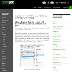
If you want to import 3D model in footprint firstly you need to open PCB library and select footprint (land pattern) on which you want to add model. After downloading 3D model from www.pcb-3d.com and selecting footprint in .pcblib, from the Altium menu, choose the option Place ->3D body. If you want to use shortcut press “pb” keyboard buttons (See Picture 1. Place ->3D body). Picture 1: Option Place ->3D body In 3D Body window in part 3D Model Type select Generic STEP Model and click on Embed STEP Model, find and select your 3D model you want to import (See picture 2. 3D Body Window).
Picture 2: 3D Body Window First position cursor in the center of footprint and then left-click will place 3D STEP (STP) model on footprint (See Picture 3. Picture 3: Place 3D body in 2D mode After placing 3D model, 3D Body window will appear again. Picture 4: Footprint view in 3D mode 1. Most downloaded models tagged with altium. Online Documentation for Altium Products. Altium Design Content. KiCad EDA Software Suite - Kicad EDA - KiCad EDA. KiCad is an EDA software suite for the creation of professional schematics and printed circuit boards up to 32 copper layers with additional technical layers.

KiCad runs on Windows, Linux and Apple OS X and is released under the open-source GNU GPL v2 free of charge. If you like KiCad or are making a good living using KiCad in your toolset, you should consider donating funds used for development. CERN has put up a place to collect donations which will be used directly to support a developer. With KiCad you can create schematic diagrams and printed circuit board up to 32 copper layers. KiCad comes with a rich set of libraries with 3D models as well.KiCad is a mature EDA software tool under active development by a team of developers and a vibrant user group. Eeschema, schematic editor.Pcbnew, printed circuit board editor, with a 3D viewer.Gerbview, Gerber file viewer. And then some other auxiliary tools: KiCad is under heavy development. STEP 1, schematic capture. STEP 3, PCB layout. KiCad EDA Software Suite - Kicad EDA - KiCad EDA. KiCad in Launchpad. Online Documentation for Altium Products. The Designator uniquely identifies each component in the design.
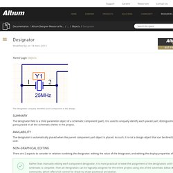
Summary The designator field is a child parameter object of a schematic component (part). It is used to uniquely identify each placed part, distinguishing it from all other parts placed in all the schematic sheets in the project. Availability The designator is automatically placed when the parent component part object is placed. Non-Graphical Editing There are 2 aspects to consider in relation to editing the designator: editing the value of the designator; and editing the display properties of the designator. Rather than manually editing each component designator, it is more practical to leave the assignment of the designators until the schematic is complete. ...via the Schematic Library Editor By default, the designator is not visible in the Schematic Library Editor.
Double click on the component name, or click the Edit button, to open the dialog and defined the value of the Designator string. Online Documentation for Altium Products. What do designers use as part of their daily arsenal in their approaches to design verification in order to be confident that their design is ready for PCB layout?
Verifying that a design is correct is often the most difficult and yet also the most important aspect during this phase. The focus of this article will be on a discussion of issues that typically cause problems for designers before the PCB layout phase, reveal strategies that can be used by the designer to avoid these pitfalls, and how Altium Designer can be leveraged to work for them. Design Verification Strategies A good strategy for design checking and debugging integrates test case design techniques into a set of well-planned series of steps that result in the successful completion of designs and delivery to market.
What you need is a roadmap for everything that will be conducted as a part of this process. The best way to approach verifying your design is to have software that gives you as much help as possible! Figure 1. Linking Existing Components to Your Company Database. This document provides detailed information on linking existing Altium Designer components to an external database using Altium Designer's database link feature.

Tip: Linking between schematic library components and an external database can only be achieved if the library is part of a library package (*.LibPkg). Choose File » New » Project » Integrated Library to create a new library package and then add the source schematic libraries to it. A common requirement for many organizations is to link from the electronic CAD components to the company's central component database. Altium Designer supports this by providing the ability to link existing components to records in the company database, through the creation and use of a database link file.