
Making an OLED. Making an OLED - Light from Carbon Compounds. LEDs and OLEDs - How it Works, Inventors. News & Events - Researchers Develop Darkest Manmade Material. January 22, 2008 Carbon nanotube array absorbs light, could boost solar energy conversion Troy, N.Y. — Researchers at Rensselaer Polytechnic Institute and Rice University have created the darkest material ever made by man.
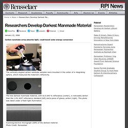
The material, a thin coating comprised of low-density arrays of loosely vertically-aligned carbon nanotubes, absorbs more than 99.9 percent of light and one day could be used to boost the effectiveness and efficiency of solar energy conversion, infrared sensors, and other devices. The researchers who developed the material have applied for a Guinness World Record for their efforts. “It is a fascinating technology, and this discovery will allow us to increase the absorption efficiency of light as well as the overall radiation-to-electricity efficiency of solar energy conservation,” said Shawn-Yu Lin, professor of physics at Rensselaer and a member of the university’s Future Chips Constellation, who led the research project.
The project was funded by the U.S. Magnetic Iron Oxide. Nanotubes +ink +paper =instant battery (18) Welcome - Bare Conductive. Infrared-Harvesting Solar Cells Made Entirely from Carbon Invented at MIT. An atomic-force microscope image of a layer of single-walled carbon nanotubes deposited on a silicon surface, as the first step in manufacturing the new type of solar cell developed by an MIT team.
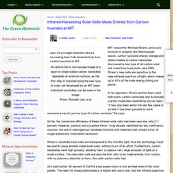
Individual nanotubes can be seen in the image.Photo: Rishabh Jain et al. DARPA: Energy Harvesting Using Rectennas. DARPA, NSF and Navy: Design and Development of Infrared Rectennas for Long Wave Infrared Imaging and Energy Harvesting Major goals of this program are to investigate, ultimately design and fabricate rectenna based systems to perform detection, communications, imaging, harvesting and control of high frequency electromagnetic radiation.
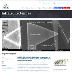
We will concentrate largely on the part of the spectrum that is not typically accessible with standard optical techniques or radio frequency (RF) electronics. In other words, we will penetrate the ‘in-between’ Terahertz region with the goal of making it an accessible part of the spectrum. The rectenna is a novel combination of a micro-antenna and a tunneling metal-insulator-metal (MIM) diode. This combination will allow for conversion of electromagnetic radiation in the terahertz frequency range (AC) directly into direct current (DC). Ultra Thin Battery. The UT Series is the industry's thinnest printed battery currently in production, with a 30 percent slimmer laminate profile (as thin as 500 microns ~ 0.020 in).

The batteries are extremely flexible and durable, even under high duty levels, and offer the same "green" advantages as the ST Series. UT batteries are available in a variety of shapes and sizes. Blue_spark_st_series_batteries_oct-12_v3.pdf. 6_William%20Ray_Nth%20Degree. White LEDs printed on paper. Lighting Sheets Made of Tiny LEDs. A company called Nth Degree Technologies hopes to replace light bulbs with what look like glowing sheets of paper.
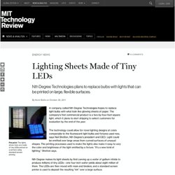
The company’s first commercial product is a two-by-four-foot-square light, which it plans to start shipping to select customers for evaluation by the end of the year. The technology could allow for novel lighting designs at costs comparable to the fluorescent light bulbs and fixtures used now, says Neil Shotton, Nth Degree’s president and CEO. Light could be emitted over large areas from curved surfaces of unusual shapes. The printing processes used to make the lights also make it easy to vary the color and brightness of the light emitted by a fixture. “It’s a new kind of lighting,” Shotton says. Conductive Adhesives for Scanning Electron Microscopy. PELCO® Conductive Liquid Silver Paint a reliable conductive ground path for SEM specimens Air drying silver paint to make effective ground.
Curable at room temperature and has high adhesion to any material. Surfaces do not have to be prepared prior to application and will adhere to such materials as polymer (phenolic) boards, ceramic, glass, metal, plastic and fiberglass. It should be mixed well with a spatula before using. RoHS compliant. The container is offered in two sizes (15g and 30g) and is provided with an applicator brush. Silver conductive ink & paste. What are Conductive Inks?
Conductive inks (also called polymer thick films) from DuPont Microcircuit Materials bring sophisticated multilayer designs within reach of virtually every membrane switch designer. All DuPont conductive inks are composed of three main components: polymer binder, conductive phase, and solvent. The polymer binder, when combined with the conductive and solvent phases, is a liquid that can be "printed" onto polyester film, forming flexible printed circuits. After printing, the solvent is evaporated out of the mixture, leaving a stable conductive pattern on the flexible substrate.
ESD Foam, Conductive Foam, Antistatic Foam & Bubble. CircuitWorks. Creative Materials Incorporated - Ag-AgCl Inks. Creative Materials' standard and custom formulations of silver-silver chloride (Ag-AgCl) inks include various ratios of silver and silver chloride.

We are able to meet specific customers' needs for sensitivity and conductivity for producing medical sensors used in biomedical monitoring, diagnostic applications and iontopheretic drug delivery. Creative Materials Incorporated - Literature. Literature Company Brochure View as pdf» Product Selector Guide View as pdf» Pad Printing Products View as pdf» Applications Guides:

Brevet US6084007 - Transparent conductive ink - Google Brevets. In the following, description will be given on embodiments of the present invention.
Toluene is used as the solvent component in the acrylic thermoplastic resin used in the embodiments. A material having the following composition was placed in a glass bottle of 1-liter volume together with 200 g of glass beads (manufactured by Toshiba-Ballotini Co., Ltd.), and this was dispersed in a paint shaker for 4 hours to have average particle size of 1 μm or less. ______________________________________Acrylic thermoplastic resin solution 100 weight parts(Copolymer resin of ethyl methacrylate and ethylacrylate; Tg 75Tin oxide powder (containing antimony pentoxide; 90 weight partsaverage primary particle size 0.2 μm)Toluene 70 weight parts______________________________________ The transparent conductive ink thus obtained was measured by toluene using Zahn cup No.3 to adjust to 20 to 25 sec. and was evaluated using sheet-fed gravure printing proof press.
Www.InkTec.com. Interested? Printed Photovoltaics. NthDegree will offer subsidy-free, grid-competitive solar energy solutions. Leveraging NthDegree’s printed semiconductor technology, we are developing a new thin-film photovoltaic device made of spherical silicon. Competitive in efficiency to conventional solar panels, Nth’s technology will have the added advantage of collecting diffuse light at normal incidence, eliminating the need for costly light tracking systems. Our lightweight and flexible design will allow efficient rooftop installation resulting in a reduced balance of system cost. NthDegree’s photovoltaic (PV) panels will be manufactured using our patented atmospheric roll-to-roll process. Conventional solar panel manufacturing facilities require substantial capital investment and ongoing manufacturing expenditures.
Nth’s combined lower manufacturing, module, and installation costs will result in a clean energy resource that has a total levelized cost of electricity competitive with utility power today. Mc10 - Conformal Electronics. Nanorods / Quantum Rods from READE. Nanorod Synonyms: nanorods, nanorod arrays, quantum rods, nanopillar, Alumina nanorods, Bismuth nanorods, Cadmium selenide nanorods, Copper nanorods, Gallium nitride nanorods, Gold nanorods, Gallium phosphide nanorods, Germanium nanorods, Indium phosphide nanorods, Magnesium oxide nanorods, Manganese oxide nanorods, Nickel nanorods, Palladium nanorods, Platinum nanorods, Silicon nanorods, Silicon carbide nanorods, Titanium dioxide nanorods, Zinc oxide nanorods, Nanorod General Definition: Nanostructures shaped like long sticks or dowels with a diameter in the nanoscale but having a length that is very much longer.
Nanorod Description: DownLoad.aspx?path=MSA20100200006_53408995. Silver Conductive Ink - Buy Conductive Ink,Silver Ink,Silver Conductive Ink Product on Alibaba. Carbon Paste Ink - Buy Carbon Paste Ink,Conductive Printing Ink For Remote Control,Carbon Paste For Membrane Switch Product on Alibaba. Printed electronics: Not just blinking beer bottles. High performance access to file storage "Printed electronics" is one of those terms one sees being bandied about without really knowing what it means or why it's important. The premise of using printing techniques to create electrical circuits isn't hard to comprehend, but not everyone agrees on what comprises a "printing technique" or why you might want to use one, so El Reg chatted to three companies at the forefront of the field. According to these firms, the new printing technique is going to change the literal fabric upon which the electronics industry rests. That's important as it's not the electronics which change as a result of the printing process, but rather the material on which those electronics rest.
Liquid X Printed Metals, Inc. Technology. T+works is the Research and Development arm of T+ink that creates the intellectual property. T+works focuses on the design and engineering of new conductive ink formulations and applications. T+ios is the primary communication platform for all T+ink enabled objects, acting as the bridge between the digital world and the physical ink.