
Diamond cubic animation - Diamond cubic. An Introduction to Photoluminescence Spectroscopy for Diamond and Its Applications in Gemology. Bidny A.S., Dolgova O.S., Baksheev I.A., Ekimenkova I.A. (2010) New data for distinguishing between hydrothermal synthetic, flux synthetic, and natural corundum. Journal of Gemmology, Vol. 32, No. 1–4, pp. 2–15.
Breeding C.M., Shigley J.E. (2009) The “type” classification system of diamonds and its importance in gemology. G&G, Vol. 45, No. 2, pp. 96–111, Mechanosynthesis of Diamond. Blogging a Crystal Structure a day in 2014. Crystal structures in material science. Software: Crystal & Molecular Structures Visualization and Diffraction. Diamond cubic. The diamond cubic crystal structure is a repeating pattern of 8 atoms that certain materials may adopt as they solidify.
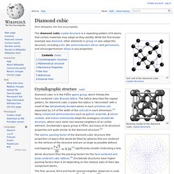
While the first known example was diamond, other elements in group 14 also adopt this structure, including α-tin, the semiconductors silicon and germanium, and silicon/germanium alloys in any proportion. Flash: 3D Crystal Viewer - ARCHIVES. Crystallographic defect. Crystalline solids exhibit a periodic crystal structure.
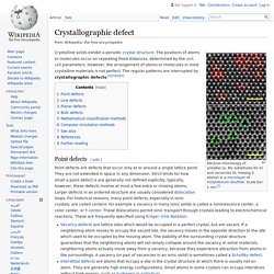
The positions of atoms or molecules occur on repeating fixed distances, determined by the unit cell parameters. However, the arrangement of atoms or molecules in most crystalline materials is not perfect. The regular patterns are interrupted by crystallographic defects.[2][3][4][5] Point defects[edit] Point defects are defects that occur only at or around a single lattice point. Vacancy defects are lattice sites which would be occupied in a perfect crystal, but are vacant. Schematic illustration of some simple point defect types in a monatomic solid A nearby pair of a vacancy and an interstitial is often called a Frenkel defect or Frenkel pair. Nitrogen in Diamonds. The main impurity found in diamonds is nitrogen.
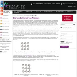
The atoms become trapped in the diamond’s crystal lattice during its natural formation, causing its natural coloring to be altered. The nitrogen can be present inside the lattice in different forms: as single atoms, as different kinds of small aggregates (2 or 3 atoms), or as larger clusters. The different forms cause the diamonds to change their spectroscopic properties, namely to have different colors by changing the light absorption and refraction/dispersion properties of the stones. It is widely agreed that the incorporation of nitrogen in the diamond structure leads to a yellow to brown color in its appearance.
Nitrogen-vacancy center. The nitrogen-vacancy center (N-V center) is one of numerous point defects in diamond.
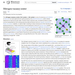
Its most explored and useful property is photoluminescence, which can be easily detected from an individual N-V center, especially those in the negative charge state (N-V−). Electron spins at N-V centers, localized at atomic scales, can be manipulated at room temperature by applying a magnetic field, electric field, microwave radiation or light, or a combination, resulting in sharp resonances in the intensity and wavelength of the photoluminescence.
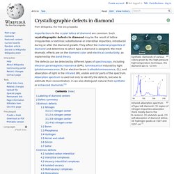
Crystallographic defects in diamond. Synthetic diamonds of various colors grown by the high-pressure high-temperature technique, the diamond size is ~2 mm Infrared absorption spectrum of type IaB diamond. (1) region of nitrogen impurities absorption (here mostly due to the B-centers), (2) platelets peak, (3) self-absorption of diamond lattice, (4) hydrogen peaks at 3107 and 3237 cm−1 Imperfections in the crystal lattice of diamond are common.
Such crystallographic defects in diamond may be the result of lattice irregularities or extrinsic substitutional or interstitial impurities, introduced during or after the diamond growth. They affect the material properties of diamond and determine to which type a diamond is assigned; the most dramatic effects are on the diamond color and electrical conductivity, as explained by the band theory. CVD-Grown Synthetic Diamonds, Part 1: History. Dating back to the 19th century, there have been many claims for creating diamond in a lab.
For many years, the conventional wisdom was that diamond would form only under conditions of high pressure and high temperature (HPHT). Indeed, the first commercially available “manmade” diamond was produced at high pressure and high temperature by General Electric in 1956. HPHT growth imitates natural diamond formation, but with carefully selected input materials to catalyze crystal growth. Today, billions of carats of diamonds are manufactured annually by the HPHT process, mostly for industrial applications.
CVD-Grown Synthetic Diamonds, Part 2: Properties. Part 1 of this series provided a brief history of CVD synthetic diamonds.
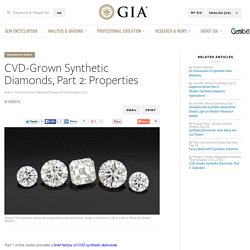
The physical properties of CVD synthetic diamond fall well within the range for natural diamonds in terms of hardness, thermal conductivity, strength, and so forth. Therefore, CVD synthetics are as hard and durable as natural diamond and display the same brilliance and fire when cut as a gemstone. CVD-Grown Synthetic Diamonds, Part 3: Detection. CVD Diamond Group - School of Chemistry - Bristol University. Welcome to the CVD Diamond Lab based in the School of Chemistry at the University of Bristol, UK.
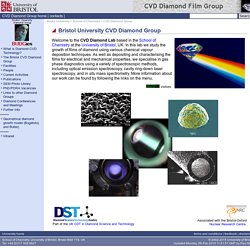
In this lab we study the growth of films of diamond using various chemical vapour deposition techniques. As well as depositing and characterising the films for electrical and mechanical properties, we specialise in gas phase diagnostics using a variety of spectroscopic methods, including optical emission spectroscopy, cavity ring-down laser spectroscopy, and in situ mass spectrometry. E6_CVD_Diamond_Handbook_A5_v10X. Chemical vapor deposition. DCplasma (violet) enhances the growth of carbon nanotubes in laboratory-scale PECVD apparatus Types[edit]
Large Colorless HPHT-Grown Synthetic Gem Diamonds from New Diamond Technology, Russia. The Russian company New Diamond Technology is producing colorless and near-colorless HPHT-grown synthetic diamonds for the gem trade.
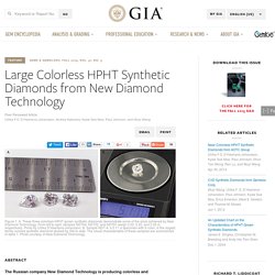
Forty-four faceted samples synthesized using modified cubic presses were analyzed using a combination of spectroscopic and gemological techniques to characterize the quality of the material and determine the means of distinguishing them from natural, treated, and alternative laboratory-grown diamonds. These samples, with weights ranging from 0.20 to 5.11 ct, had color grades from D to K and clarity grades from IF to I2. Importantly, 89% were classified as colorless (D–F), demonstrating that HPHT growth methods can be used to routinely achieve these color grades. Infrared absorption analysis showed that all were either type IIa or weak type IIb, and photoluminescence spectroscopy revealed that they contained Ni-, Si-, or N-related defects. HPHT Diamonds. Submit the diamonds to be HPHT processed to our office in New York City.
Our in-house experts will inspect the diamonds to determine the suitability of the stone for the process. The expected results will be communicated to the client. At this point we require clients final approval and acceptance of our terms to process the diamond. On client's approval, the diamond is submitted to our lab for HPHT processing. This process usually takes 10 to 15 business days. To submit a stone for processing please ship it to our New York address.
Pricing for the HPHT process depends on the specific needs. Material properties of diamond. Hardness and crystal structure[edit] Molar volume vs. pressure at room temperature. Visualisation of a diamond cubic unit cell: 1. Components of a unit cell, 2. Properties of Diamond, Silicon and Germanium. Dielectric.
A polarized dielectric material The study of dielectric properties concerns storage and dissipation of electric and magnetic energy in materials.[2] Dielectrics are important for explaining various phenomena in electronics, optics, and solid-state physics. Terminology[edit] While the term insulator implies low electrical conduction, dielectric typically means materials with a high polarizability. The latter is expressed by a number called the relative permittivity (also known in older texts as dielectric constant).
The term insulator is generally used to indicate electrical obstruction while the term dielectric is used to indicate the energy storing capacity of the material (by means of polarization). Electric susceptibility[edit] Main article: permittivity. Synthetic Diamonds: Improved Quality and Identification Challenges. Diamond type. Different diamond types react in different ways to diamond enhancement techniques. Different types can coexist within a single stone; natural diamonds are often mixes of Type Ia and Ib, which can be determined by their infrared absorption spectrum.[2] Type I diamonds, the most common class, contain nitrogen atoms as their main impurity, commonly at a concentration of 0.1%.
Type I diamonds absorb in both the infrared and ultraviolet region, from 320 nm. Epitaxy. "Epitaxis" redirects here. It is not to be confused with Epistaxis. The overlayer is called an epitaxial film or epitaxial layer. The term epitaxy comes from the Greek roots epi (ἐπί), meaning "above", and taxis (τάξις), meaning "an ordered manner". It can be translated as "arranging upon". For most technological applications, it is desired that the deposited material form a crystalline overlayer that has one well-defined orientation with respect to the substrate crystal structure (single-domain epitaxy). Diamond color. Possible colors[edit] Diamond. Allotrope of carbon often used as a gemstone and an abrasive.
Synthetic diamond.