
Experiments demonstrate nanoscale metallic conductivity in ferroelectrics. The prospect of electronics at the nanoscale may be even more promising with the first observation of metallic conductance in ferroelectric nanodomains by researchers at Oak Ridge National Laboratory.
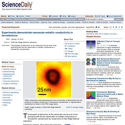
Ferroelectric materials, which switch their polarization with the application of an electric field, have long been used in devices such as ultrasound machines and sensors. Now, discoveries about ferroelectrics' electronic properties are opening up possibilities of applications in nanoscale electronics and information storage. In a paper published in the American Chemical Society's Nano Letters, the ORNL-led team demonstrated metallic conductivity in a ferroelectric film that otherwise acts as an insulator. Nanowires enable faster, low-power 10nm 3D transistors.
Faster organic semiconductors for flexible displays can be developed quickly with new method. By Louis Bergeron Anatoliy Sokolov A single crystal of the new organic semiconductor material shown in polarized light.
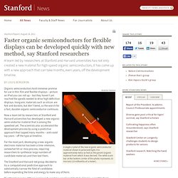
It is approximately twice as fast as the parent organic material from which it was derived. The white scale bar at the bottom center of the photo represents 10 microns (10 millionths of a meter). Organic semiconductors hold immense promise for use in thin film and flexible displays – picture an iPad you can roll up – but they haven’t yet reached the speeds needed to drive high definition displays. Now a team led by researchers at Stanford and Harvard universities has developed a new organic semiconductor material that is among the speediest yet.
3-D Printer with Nano-Precision. German scientists build world's smallest steam engine using lasers. For those of you out there that are in love with fuel efficient vehicles, German scientists at the Max Planck Institute for intelligent systems have created the world’s smallest steam-powered engine out of a couple of lasers and a tiny colloid ball.

Imagine being able to power your Prius with a bank of microscopic steam engines, you would be the envy of all your green friends! The researchers took the original model of the steam engine built by Robert Stirling almost 200 years ago and miniaturized the process in which it generates power. Emulating the traditional method of using expanding and contracting gases to power a piston, they installed a modulating laser to do the work in the minuscule machine.
Multiferroics could lead to low-power devices. Born to be Viral: Watch a surgical robot peel a grape. MacGregor Campbell, consultant.
Atoms to X-Rays: Sensing with Nanomaterials. Berkeley creates flexible, rugged, plastic electronic skin with carbon nanotubes. Using semiconductor-enriched carbon nanotubes, researchers from the Department of Energy’s Berkeley Lab have pioneered a technique for creating large-scale, flexible, inexpensive, thin-film transistor “electronic skin.” These stretchy, rugged sheets are the first step in creating wearable computers, intelligent sensors that can treat infections, and computers/books that can be folded up into a jacket pocket. A carbon nanotube, like graphene, is flexible and strong, and thus an ideal candidate for flexible transistors — but naturally forms into two forms, one of which is metallic, the other a semiconductor. This mixture can be used to make thin-film transistors, but its not as conductive, and thus not as useful.
To make the electronic skin, the Berkeley researchers had to purify a solution of carbon nanotubes so that 99% were the semiconductor form. On the other hand, plastic circuits are incredibly exciting to medical professionals, too. Flexible nanowire electronics that can attach to any material developed at Stanford. Stanford researchers have developed a new method of attaching nanowire electronics to the surface of virtually any object, regardless of its shape or what material it is made of.
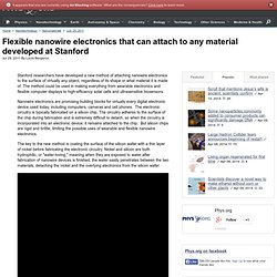
The method could be used in making everything from wearable electronics and flexible computer displays to high-efficiency solar cells and ultrasensitive biosensors. Nanowire electronics are promising building blocks for virtually every digital electronic device used today, including computers, cameras and cell phones. The electronic circuitry is typically fabricated on a silicon chip.
The circuitry adheres to the surface of the chip during fabrication and is extremely difficult to detach, so when the circuitry is incorporated into an electronic device, it remains attached to the chip. But silicon chips are rigid and brittle, limiting the possible uses of wearable and flexible nanowire electronics.
Currently her team has been working with polymer layers about 800 nanometers thick. NASA creates groundbreaking super black light absorbing material. 0.03-inch wide close-up of the super-black, carbon nanotube coating Even though NASA has drastically scaled back its missions into space, that doesn’t mean the agency has stopped research for the benefit of space exploration.

Evidence of this comes in the form of a new, super-black material that just got unveiled during the SPIE Optics and Photonics conference. NASA is claiming it is the most light absorbent material ever developed, and capable of absorbing 99% of ultraviolet, infrared, far-infrared, and visible light. That may not sound too impressive on its own until you find out what it can be used for and the benefits it brings. The super-black material is about 10,000 times thinner than a human hair and created using carbon nanotubes. The resulting coated materials offer up some major advantages over existing light absorption techniques used on instruments bound for space. Read more at NASA. New kind of high-temperature photonic crystal could someday power everything from smartphones to spacecraft.
A team of MIT researchers has developed a way of making a high-temperature version of a kind of materials called photonic crystals, using metals such as tungsten or tantalum.
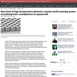
The new materials — which can operate at temperatures up to 1200 degrees Celsius — could find a wide variety of applications powering portable electronic devices, spacecraft to probe deep space, and new infrared light emitters that could be used as chemical detectors and sensors. Compared to earlier attempts to make high-temperature photonic crystals, the new approach is “higher performance, simpler, robust and amenable to inexpensive large-scale production,” says Ivan Celanovic ScD ’06, senior author of a paper describing the work in the Proceedings of the National Academy of Sciences. The paper was co-authored by MIT professors John Joannopoulos and Marin Soljačić, graduate students Yi Xiang Yeng and Walker Chen, affiliate Michael Ghebrebrhan and former postdoc Peter Bermel.
Self-healing circuits fix themselves after damage. University of Illinois engineers have developed a way of automatically restoring electrical conductivity to a cracked circuit in less time than it takes to blink.
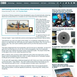
With chip density increasing all the time, reliabilty is becoming more of an issue - there's simply more to go wrong. But the new material means that when a circuit cracks or fails, the chip can simply fix itself. "In general there's not much avenue for manual repair," says materials science and engineering professor Nancy Sotto.
"Sometimes you just can't get to the inside.