
Graphene acts as plasmonic antenna, leads towards 0.1nm wires in chips. Are you sick of graphene-related breakthroughs yet?
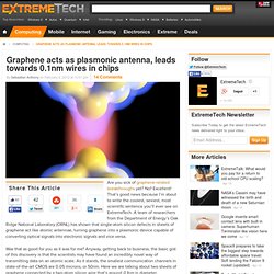
No? Excellent! That’s good news because I’m about to write the coolest, sexiest, most scientific sentence you’ll ever see on ExtremeTech. Graphene electronics moves into a third dimension. Wonder material graphene has been touted as the next silicon, with one major problem -- it is too conductive to be used in computer chips.

Now scientists from The University of Manchester have given its prospects a new lifeline. In a paper recently published in Science, a Manchester team lead by Nobel laureates Professor Andre Geim and Professor Konstantin Novoselov has literally opened a third dimension in graphene research. Their research shows a transistor that may prove the missing link for graphene to become the next silicon. First inkjet-printed graphene computer circuit is transparent, flexible. You can add another crazy characteristic to graphene’s ever-expanding list of “wonder material” properties: It can now be used to create flexible, transparent thin-film transistors… using an inkjet printer.
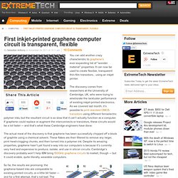
The discovery comes from researchers at the University of Cambridge, UK, who were trying to ameliorate the lackluster performance of existing inkjet-printed electronics. As we covered last month, it’s possible to print standard CMOS transistors using different ferroelectric polymer inks, but the resultant circuit is so slow that it can’t actually function as a computer.
If graphene could replace or augment the interconnects or transistors, these circuits would be a lot faster — and that’s what these Cambridge engineers have done. The actual meat of the discovery is that graphene has been successfully chipped off a block of graphite using a chemical solvent. These flakes are then filtered to remove any larger, print head-clogging chunks, and then turned into a polymer ink. Graphene: The perfect water filter. Researchers from the home of graphene, the University of Manchester in England, have discovered — seemingly by chance — one of the most important properties of graphene yet: It’s impermeable to everything but water.
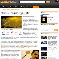
It is the perfect water filter. In an experiment, the University of Manchester researchers filled a metal container with a variety of liquids and gases and then covered it with a film of graphene oxide. Their most sensitive equipment was unable to register any molecules leaving the container, except water vapor. The graphene oxide filter even prevented helium gas from escaping, which is notoriously finicky. Graphene Competitor Used to Make Circuits. New material on the block: Atom-thick sheets of molybdenite at the end of these gold leads act as transistors.
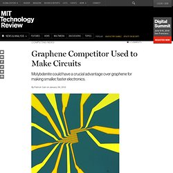
The first logic circuits made using atom-thick sheets of a material called molybdenite suggest a possible new solution to the problem of getting more power out of silicon computer components. It also establishes molybdenite as a competitor to graphene, the atom-thick sheets of carbon believed capable of solving silicon’s shortcomings, and whose creators received a Nobel prize in 2010. Silicon technology is in trouble because, for years, performance has been improved by shrinking the size of the features on silicon chips, but there is only so much more shrinking that can be done. Chips will go on sale this year with features as small as 22 nanometers, and at very small scales, silicon technology faces problems like oxidation, which reduces performance and causes energy losses. New method of growing high-quality graphene promising for next-gen technology. Public release date: 17-Oct-2011 [ Print | E-mail Share ] [ Close Window ] Contact: Melissa Van De Werfhorstmelissa@engineering.ucsb.edu 805-893-4301University of California - Santa Barbara (UC Santa Barbara) – Making waves as the material that will revolutionize electronics, graphene – composed of a single layer of Carbon atoms – has nonetheless been challenging to produce in a way that will be practical for innovative electronics applications.
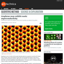
Researchers at UC Santa Barbara have discovered a method to synthesize high quality graphene in a controlled manner that may pave the way for next-generation electronics application. "Our process has certain unique advantages that give rise to high quality graphene," says Banerjee. Using adhesive tape to lift flakes of graphene from graphite, University of Manchester researchers Geim and Novoselov were awarded the 2010 Nobel Prize in Physics for their pioneering isolation and characterization of the material. According to Dr. Graphene may exhibit exotic superconductivity. Graphene is a form of carbon with enough interesting electronic properties to merit the 2010 Nobel Prize in Physics, which was awarded to Andre Geim and Konstantin Novoselov for their work in isolating and characterizing graphene.
Although its very simplicity—it's a sheet of carbon a single atom thick—can limit its applications, Rahul Nandkishore, L. S. Levitov, and A. V. Graphene creates electricity when struck by light. Oh graphene!

The cheap, easy-to-manufacture one-atom-thick sheet of carbon can add yet another weird, fantastical, and possibly life-changing ability to its list of characteristics: it has an incredibly sensitive thermoelectric response to light. In layman’s terms: graphene, when struck by light of almost any wavelength, can produce an electric current.
The discovery was made by a team of researchers from MIT in the US and the National Institute for Materials Science in Japan. A sheet of graphene was treated so that it had two regions with different electrical properties (a p-n junction). Then, by shining an 850nm infrared laser on the material a temperature difference between the two regions is created, and an electrical current flows. Now, this is significant because a hot carrier response has only ever been observed in materials that are reduced to (almost) absolute zero, or when an intensely powerful laser is used to heat the material. Frustration inspires new form of graphene. They're the building block of graphite -- ultra-thin sheets of carbon, just one atom thick, whose discovery was lauded in 2010 with a Nobel Prize in Physics.
The seemingly simple material is graphene, and many researchers believe it has great potential for many applications, from electronic devices to high-performance composite materials. Giant flakes make graphene oxide gel. (PhysOrg.com) -- Giant flakes of graphene oxide in water aggregate like a stack of pancakes, but infinitely thinner, and in the process gain characteristics that materials scientists may find delicious.

A new paper by scientists at Rice University and the University of Colorado details how slices of graphene, the single-atom form of carbon, in a solution arrange themselves to form a nematic liquid crystal in which particles are free-floating but aligned. That much was already known. The new twist is that if the flakes – in this case, graphene oxide – are big enough and concentrated enough, they retain their alignment as they form a gel. That gel is a handy precursor for manufacturing metamaterials or fibers with unique mechanical and electronic properties.
The team reported its discovery online this week in the Royal Society of Chemistry journal Soft Matter. "Graphene materials and fluid phases are a great research area," Pasquali said. Graphene supermaterial goes superpermeable: Can be used to distill alcohol. Graphene transistors compatible with living cells. A team at at the Technische Universitaet Muenchen says it's built the foundation for devices to communicate directly with the human brain.
The researchers' new graphene-based transistor array is compatible with living biological cells and can, for the first time, record the electrical signals they generate. Silicon's problematic for use with living cells - it doesn't take well to getting wet, for example, and it's expensive. However, the scientists say that graphene, which is is chemically stable and biologically inert, offers outstanding electronic performance, can easily be processed on flexible substrates, and should lend itself to large-scale, low-cost fabrication.
The researchers started with an array of 16 graphene solution-gated field-effect transistors (G-SGFETs) fabricated on copper foil by chemical vapor deposition and standard photolithographic and etching processes. "The sensing mechanism of these devices is rather simple," says Dr Jose Antonio Garrido. Researchers enhance graphene to enable multicolor photodetection. (PhysOrg.com) -- Graphene, a one-atom–thick layer of carbon lattice with a honeycomb structure, is seen as an attractive semiconductor material for use in future electronics and optoelectronics because of its speed, transparency, flexibility and strength. Recent studies have demonstrated its potential in solar cells, touch panels, ultra-fast lasers and optical modulators. And while graphene has the potential for wideband, high-speed photodetection — the sensing of light or other electromagnetic energy — it is currently hampered by its low external sensitivity to light and its inability to differentiate different colors of light.