
Charles Taylor
I am here to create friends and huge network where i can learn about the technology, semiconductors, product design which will be helpful in my work profile and self knowledge.
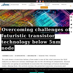
Overcoming challenges of futuristic transistor technology below 5nm node. The ‘Semiconductor era’ started in 1960 with the invention of the integrated circuit.
ASIC/FPGA based Product Design Service Company in USA - eInfochips (An Arrow Company) Top 10 Contributing Factors to Design-for-Manufacturability (DFM) Manufacturing is one of the key factors which determines product success, as it directly refers to product quality and availability. Design for Manufacturability (DFM) determines the process of ensuring optimum production efficiency and quality while taking care of potential product problems in the design phase itself. DFM saves on time; cost and effort related to product redesigning process and carves out best-manufacturing output efficiently. It takes care of factors which might impact product manufacturing including the nature of raw material, its physical and chemical attributes and its availability for faster production. Design, Integration, Verification & Validation Services. The demand for high performance, low power consumption, and low form-factor designs has dramatically increased in the past few years.
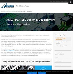
With 20+ years of experience, eInfochips helps its client in custom design and development of ASIC, FPGA, and SoCs for various industries, including Aerospace, Automotive, Networking, Consumer Electronics, Industrial, Medical, IoT, etc… With strong expertise in Mixed-signal solutions across design, verification, physical design, and validation, eInfochips specializes in lower geometry designs and have taped-out 200+ silicons, from 180nm to 7nm & beyond. We are the 1st engineering services company that has started working on 7nm and 10nm technology node.
We also offer DFT / DFM services, including architecture definition and implementation, FPGA to ASIC conversion, pre- silicon validation, post- silicon validation and yield analysis. Top 5 Solutions for Optimal DFT in Lower Technology Nodes. Design for Testability (DFT), is one of the effective ways to overcome power consumption challenges and huge data volumes in the testing process after production, which has grown dramatically in lower geometry node designs.
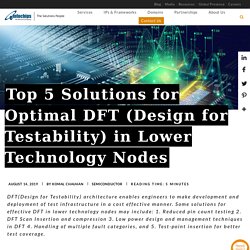
DFT is becoming a key factor that saves higher design cost, higher power consumption, increasing execution testing time, chip area, pin counts, and other new fault types at small geometries in the testing phase itself. DFT architecture approach is very easy to deploy, and also accelerates the development of a higher-quality test infrastructure at a lower cost. The advanced built-in technology enables testability for analog and mixed signal designs with limited digital inputs.
Let’s understand how the below mentioned parameters optimize the DFT architecture to overcome challenges (including timing, area, and power): 1. 3D Handheld Scanner Design. Why can’t the Semiconductor Industry afford to take its Eyes off SerDes? In this era of pervasive connectivity, everything needs to communicate with each other and everything around them by means of the internet.

There is never-ending demand for advanced integrated communication in different industry verticals such as Automotive, Consumer Electronics, IT and Telecom. And, it is getting difficult to meet an exponentially growing demand for moving data, faster than ever. SoC Functional verification flow. How to Check Signal Drive Strength in SystemVerilog. In this blog, we will showcase how signal drive strength can be checked in SystemVerilog for best possible results, and the various rules which have to be observed in “documenting” signal strength. According to basic principles of testing electronic systems, signal drive strength is considered one of the key metrics of signal integrity (SI). Whether you’re designing PCB, SoC, microcontroller, USB or any other electronic component, the ability to transmit the signal with high fidelity depends on signal drive strength.
Drive strength can be used to resolve which value should appear on a net or gate output. In a SystemVerilog test bench, it often happens that multiple drivers would try to drive a single net or output of gate. In this scenario, the output value is best determined based on the signal driving strength of each driver and its corresponding value. Pre to Post Silicon Validation, Verification, Testing Services. eInfochips has proven excellence in handling turnkey design verification testing, ODCs for semiconductor product companies across the globe. eInfochips (An Arrow Company) has well-defined methodologies that ensure design verification and validation testing effectiveness.

With our stringent process checklists, we have identified 100+ defects from market-proven Design and Verification IPs. Our team has experience in building modular and reusable verification environment. eInfochips is one of the very few companies to have a successful partnership with all leading EDA companies and has early access to the latest tools and methodologies. ASIC Design Flow in VLSI Engineering Services – A Quick Guide. Today, ASIC design flow is a very mature process in silicon turnkey design.
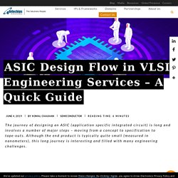
The ASIC design flow and its various steps in VLSI engineering that we describe below are based on best practices and proven methodologies in ASIC chip designs. This blog attempts to explain different steps in the ASIC design flow, starting from ASIC design concept and moving from specifications to benefits. Why to adopt the ASIC design flow? A Heuristic Approach to Fix Design Rule Check (DRC) Violations in ASIC Designs @7nm FinFET Technology. The intent of this paper is to explain the varied kinds of DRCs (Design Rule Checks) that are encountered in the Physical Design flow.

This paper will discuss the Metal DRC violations (7nm Technology) generally seen at the block level and outline the practical approach to fix them. I. Introduction Most of the VLSI engineers are aware of DRC and appreciate the need for a DRC cleaned database. This paper will give a brief idea about the different types of DRC violations, the reasons for their occurrence in the physical design, and the heuristic approach to fix it. Global Technologies & Science — Are you facing challenges in FPGA to ASIC... Physical design services expert - Industrial DFM / DFT Solutions in IoT.
With a proven physical design flow, methodologies, and with dedicated subject matter experts, eInfochips has provided RTL to GDSII service to many clients for successful Silicon tapeouts.
We were the 1st engineering services company to tapeout multiple 16nm SoC’s and at present we are working on 10nm and 7nm technology node. These SoC’s have 300 million to 500 million gates (~25*25 mm) and was developed with the focus on reducing the die size and power. We have recently started working on 10nm as well. Model-Based Design for Embedded Software - eInfochips. Model-based design (MBD) is a framework used in virtual prototyping of embedded software.

MBD has evolved to overcome various difficulties and complexities that typically arise during the design lifecycle of embedded software for closed-loop control systems. Such software needs to be designed in an iterative manner with extensive involvement of multi-disciplinary teams. In most practical scenarios, the need for embedded software design has to start early (as well as tested) before physical prototypes and systems are made available.
Using traditional design processes, the discovery of design and requirements errors found late in the design cycle can lead to expensive delays. PCB Board and Embedded Systems Design Services. The Hardware design is a critical aspect of any electronic product success, as there is a need for efficient and sleek enclosures which would appeal to end user aesthetic sensibilities and functional requirements.

Silicon Tape-out Solutions across Lower Geometry Design Layout. Need FPGA design expertise for IoT product development? SoC Functional Verification Flow. 1. SoC Level/Top Level view (Feature Extractions) During SoC verification, you must view the design at the top level and extract its SoC level functionality/features during specification study phase for its verification. At this stage, a thorough understanding of SoC functionality and its architecture is required because misunderstanding of the specification can become the leading cause of bugs, and due to this, you may waste unnecessary time on issues which are not real RTL problems. 2.
SoC Level Verification Plan Define a Clear Line Between SoC and IP: During the development of the SoC level verification plan, you have to clearly define/identify the functionalities, which needs to be verified at the SoC level and at the sub-block or sub-IP or sub-cluster level. 3. The SoC level verification environment contains sub-block level verification components/environment along with dedicated SoC level verification components/environment. [forminator_poll id=”8858″] 4. A Step-by-Step Guide to Understanding Product Engineering Services. Innovation in Learning and teaching with digital technology. Hardware Design for Internet of Things - Electronic Point of Sale (EPOS) Design Hardware Design Considerations - Top 10 Contributing Factors to Design-for-Manufacturability (DFM) -
Top 10 Contributing Factors to Design-for-Manufacturability (DFM) - 55 Semiconductor & Electronic Design Websites and Profiles to Follow in 2018. The Sky Is the Limit in 5G Game of Drones. 5G is supposed to provide effective machine-to-machine communications for robots, sensors, healthcare, smart meters, cameras, cars, drones and so on — all with different demands. It is said that 5G will empower the universal boom for entertainment, research, and business. In addition, 5G will meet the demands of many industries – including consumer electronics, avionics, IoT, etc. to name a few. However, the “one-size-fits-all” network solution is no longer applicable for all use cases and services to every device, everywhere. Experience Smart Fitness with Augmented Reality and Virtual Reality.
A Step-by-Step Guide to Understanding Product Engineering Services. It’s a deeply held belief among entrepreneurs as well as established industry leaders that early adopters of any new technology trend are more likely to succeed in that space later, as they have already worked hard to create innovative offerings that can disrupt, and dominate afterward. We all may agree that timely investment in the right business technology, for example, Internet of Things (IoT), is a recipe for long-term growth and success. However, many companies are hesitant to explore new technologies, as they do not have the required experience. On the other hand, getting engineering teams onboard with new technology adoption requires work. As soon as the rubber hits the road, there will be a lot of uncertainty factors that can create challenges and slowdowns, discouraging even the most ardent, techno-enthusiast companies from making their mark in a given technology arena.
UVM-MS Verification Framework for Mixed Signal SoC - eInfochips. NASA Just Dropped Its Most Detailed Video Tour of the Moon Yet. eInfochips: ARM Approved Design Partner. End-to-End ASIC Design Solution for Shorter TTM - ELE Times. Physical Design Services. eInfochips Strengthens RTL-to-GDSII Design Service Capabilities, Adopts Magma IC Implementation Flow. eInfochips helps to deal with ASIC Design & FPGA - SoC Verification Services. Www.einfochips. The Sky Is the Limit in 5G Game of Drones. Semiconductors & More Than Moore. SemiConductors. Analog Mixed Signal Verification Methodology (AMSVM)
Common Challenges of Lower-Technology Nodes for IoT Devices. In 1965, Gordon Moore, a co-founder of Intel, observed that the number of transistors per square inch on integrated circuits has doubled approximately every two years since the IC was invented. This is known as Moore's law, and it has helped in the evolution of smaller, cheaper, more powerful devices, which has led to consumers taking computing technologies for granted. As the semiconductor industry races toward lower-technology nodes, the focus now is on more powerful chips with reliable Internet of Things (IoT) support. Considering this, the IoT has become a mainstream technology for companies looking to accelerate the growth of chip connectivity in the upcoming years.
Moreover, with the emergence of the IoT, the semiconductor industry has an opportunity to use Moore's law to deliver computing capabilities that can support Internet-connected devices like desktops, smartphones and wearables. Comparison between Qualcomm® Snapdragon™ Platforms - 212 (APQ8009), 410E (APQ8016), 600E (APQ8064), 625 (APQ8053) and 820 (APQ8096) - Product Engineering Blog.
Since its inception in 1985, Qualcomm® is engaged in the design, development, manufacturing and commercialization of digital telecommunications products and services. According to the report of Insight Research Corp. in 2006, the worldwide telecom industry was in growth mode and its revenue was predicted to climb to $1.3 trillion by 2007. To grab that opportunity, Qualcomm® launched Snapdragon™ system on chip (SoC) in November 2006 by including scorpion processor and other required semiconductors in it.
By July 2007, Qualcomm® named as world’s leading mobile integrated circuits (chipsets) provider by market research firm iSupply. Cloud Operations and Continuous Monitoring - Product Engineering Blog. IT operations management (ITOM) and IT operations analytics (ITOA) help an organization ensure consistency, reliability and quality of services. Latest IT trends affecting IT operations include cloud computing, machine-to-machine (M2M) communications and the Internet of Things (IoT).
IT operations are mainly concerned with various procedures and services administered and monitored by an organization’s information technology (IT) department. They include administrative processes and support for hardware and software, catering to internal as well as external clients. The main prerequisite of IT operations is that they should be capable of delivering effective services at a given desired quality and cost.
Q&A on ASIC-FPGA-SoC Design and Solutions - Product Engineering Blog. 1. Improving DevOps Success with Well-Defined Metrics - DevOps.com. Challenges and Opportunities for the Semiconductor Industry in the IoT. The Internet of Things has become a mainstream technology strategy for businesses looking to accelerate growth in 2017 and beyond. The semiconductor industry isn't immune to the ongoing IoT buzz, as experts believe that major players will soon abandon the pursuit of Moore's Law in favor of a wholesome strategy necessitating more powerful chips and reliable IoT applications—an important enabler to a connected world. So, what explains the draw to IoT movement?
Most semiconductor companies are motivated by the pursuit of an increased foothold in the technology space, as well as stronger customer relationships that will be fostered owing to their ability to deliver unparalleled customer experiences through IoT solutions. Product Engineering Blog. 1. How do you define DevOps? DevOps is a clipped compound term which combines “Development” and “Operations” practices of IT software development, having originated in the mid 2000s among IT professionals looking for efficient and innovative ways to automate and speed up the process of software delivery. As a change agent, DevOps promotes a culture of collaboration and information sharing across the organization, a radical departure from the ‘silos’ of the past.
Correlation of Routability and Placement Density for better QoR in 16nm technology. Custom Design SoM / SBC based on Qualcomm® Snapdragon™ 212 (APQ8009), 410, 600, 625(APQ8053) and 820 processors. Q&A on ASIC-FPGA-SoC Design and Solutions. 1. UVM Verification Framework for Optical Network SoC - eInfochips. An introduction to ARM Cortex-M0 DesignStart. Komal Chauhan on Flipboard.
SoC Verification - eInfochips. DevOps in IT versus DevOps in Internet-of-Things. In our last post on How DevOps drives business in PES, we briefly touched on the key differences between DevOps for connected devices and DevOps for pure play IT. It was shown that when it comes to product engineering, the physical component and existing legacy systems add an extra layer of complexity to the overall automation process.
In this post, we will elaborate further on the key differences between DevOps in IoT companies and pure play IT, and the specific challenges that teams working in IoT and connected devices are trying to address to achieve a smooth transition to DevOps methodology. Development Pipeline. Design Rule Checks (DRC) - A Practical View for 28nm Technology. Physical Design on TSMC's 16nm FinFET for SDN - eInfochips. Consulting, Implementation, CloudOps. Intelligent Vending Machine - Controller Design - eInfochips.
RTL to GDSII Turnkey ASIC for MEMS Applications - eInfochips. PLCs, PICs, and SBCs. Semiconductor. Achieving Verification Excellence through Universal Verification Methodology (UVM) - Examlysis. Pokémon GO Season in Full Swing: Does your Smartphone Performance Measure up? The Role of Snapdragon 820 in 4k Ultra HD Technology – eragon by eInfochips. Top Tips to Enhance Design For Testability (DFT) for Semiconductors Industry. Fly a Drone! Best Tips for Enhancing the Efficiency of Automated Testing - All. Escaping Technical Debt With Agile Methodology - DZone Agile. How to 'Productize' Your Service Business Offerings. Some Cool Tips For The White Balance Eyedropper Tool.
Brian May launches smartphone adapter for stereoscopic virtual reality viewer: Digital Photography Review. Sugar - I Had No Idea. Cool tricks with magnets and marbles.
Empower the Customer with Superior Quality Products through QA & Test Automation — Medium.
This going to be very helpful to qa testing team in an easy way. – alexispeck73
DO-254, DO-178B/C, DO-160, ARP-4754 with all levels of SOI Certification.
This is tremendous platform to make Avionics field rise to the new level. Good going!! – alexispeck73
Innovator and wind-flow software developer, Liz Walls. Jefferson 3-D images software developer Scandy gets $1 million in funding. Get Freescale i.MX6 Development Boards & Kits at eInfochips. Order Now!! Data Analytics, Visualization & Reporting Services. Latest Trends Shaping the Direction of Security and Surveillance Market. 10 Of The Coolest Gadgets We Saw At CES 2016. Security, Surveillance & Access Controls: Network/Digital Video Recorder Video Surveillance Evolving Trends. CBP Picks Telephonics Mobile Surveillance Vehicles for Border Security; Joseph Battaglia Comments. Influencing Trust for Human-Automation Collaborative Scheduling of Multiple Unmanned Vehicles. - Abstract. ASIC Product Design and Development. Ecommerce softwares. Semiconductor News. Aerospace & Defence. Technologies.