
From the CAD Library: Padstacks. Padstack creation is something every CAD tool will eventually have to incorporate because it expedites and optimizes the constructionof CAD libraries.
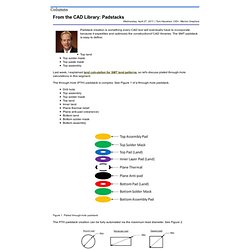
The SMT padstack is easy to define: Top landTop solder maskTop paste maskTop assembly Last week, I explained land calculation for SMT land patterns, so let's discuss plated through-hole calculations in this segment. The through-hole (PTH) padstack is complex. See Figure 1 of a through-hole padstack. Drill holeTop assemblyTop solder maskTop landInner landPlane thermal reliefPlane anti-pad (clearance)Bottom landBottom solder maskBottom assembly Figure 1. The PTH padstack creation can be fully automated via the maximum lead diameter. Figure 2. IPC-2222 Table 9-3 has a hole size calculation chart for maximum lead + level = minimum hole size. IPC-2222, Table 9-3. Once you calculate the hole size, add the minimum annular ring of 0.05 mm per IPC-2221 Table 9-2. Figure 3.
IPC-2221, Table 9-1. Figure 4. Producibility Levels IPC Performance Classifications. Printed Circuit University.
SCHEMATIC. STANDARDS & TESTING. Fiducial Mark Requirements. Free 3D Models, Free CAD Models. About PCB Panels for Manufacturing. Control PCB Fabrication Costs by Thinking About Panel Sizes Getting the most for your money in custom printed circuit board manufacturing requires a little up-front knowledge of how they are made.
Unfortunately, your manufacturing partner may not talk completely straight about their processes and pricing model (kudos to those that have live pricing on the websites). If you're new to the industry, or just looking for hints on how to lower your PCB costs, keep reading and perhaps you'll learn something new. Nothing in this article is rocket-science, it's really a matter of some common-sense math. While designed-in features are the predominant driver of PCB manufacturing costs, the more subtle factor of panelization efficiency can also have a dramatic impact. The second key thing to understand is that the cost of manufacturing panels is basically fixed for a given set of technology. The math behind finding the best board size isn't complex, but it's tedious. 5 x 3.1 5.25 x 3.45 3.45 x 5.25. Practical Electronics/PCB Layout. The efficient laying out of traces on a PCB is a complex skill, and requires much patience.

This task has been made vastly easier with the advent of readily available PCB layout software, but it is still challenging. Usually an electronics or electrical engineer designs the circuit, and a layout specialist designs the PCB. PCB design is a specialized skill. There are numerous techniques and standards used to design a PCB that is easy to manufacture and yet small and inexpensive. Copper Thickness[edit] The vast majority of PCBs are manufactured with "1 ounce copper" on the outer layers. The thickness of the copper layer on the PCB affects the behaviour of the circuit. As always, the thickness of a thin slab of metal with a given top surface area is always exactly The area is "1 square foot" (144 square inches), the density of copper is 8.96 mg/mm3 = 5.18 ounce/(inch3), and usually the mass is "1 ounce of copper", but occasionally 1/2, 2, 3, or 4 oz.
Trace Width[edit] [edit] Holes[edit]