
Wire Gauge calculations. PCB Design from Black Stick Ltd. Via Calculators Via Current Carrying Capacity The Via current carying calculator allows you to work out current carying capcity of a via and is based on the IPC-2152 - "Standard for Determining Current Carrying Capacity in Printed Board Design".

Track Width Calculators Track Current Carrying Capacity The track width calculator allows you to work out current carying capcity of a track and is based on the IPC-2152 - "Standard for Determining Current Carrying Capacity in Printed Board Design". Other Calculators C4 calculator Our C4 calculator is a downloadable aplication that allows you to calculate the current carrying capacity of tracks and vias as well as voltage gap seporation of condudtors, and is based on the IPC-2152.
We will be adding more calculators soon. Differential Pair Calculator. The Saturn PCB Toolkit is the best resource for PCB related calculations you can find.

It incorporates many features that PCB designers and engineers are in regular need of like current capacity of a PCB trace, via current, differential pairs and much more. Please download our PCB Toolkit today for free and enjoy! Download Version 6.64 Now! Help keep the Saturn PCB Toolkit free by making an online donation today! In order to understand the PCB Toolkit version differences, I have added this brief description of the version series. ANSI PCB Track Width Calculator. This is the NEW version of my calculator.

The original version is HERE. New features in this version include: use of metric or imperial units for all major fields the ability to change units for any applicable field on the fly minor enhancements to some of the calculations - IPC-2221(A) changes the curve fit saving of all parameters in a cookie to keep your preferences between visits This page calculates approximations to the ANSI / IPC-2221/IPC-2221A design standards for PCB trace width - this is the replacement for IPC-D-275. The approximations and rationale are described in Temperature Rise in PCB Traces, equations 13 & 15. by Douglas Brooks, UltraCAD Design, Inc.
The figures returned by this calculator are to be taken as a guide only. The trace width formulas are: Internal traces : I = 0.024 x dT0.44 x A0.725 External traces: I = 0.048 x dT0.44 x A0.725 where: I = maximum current in Amps dT = temperature rise above ambient in °C A = cross-sectional area in mils² From the CAD Library: Inch-to-Metric Conversion Tables. How to Move Forward Let’s start the transition process.

Fully 99% of all PCB layouts use vias. See Table 2 for an inch to millimeter conversion chart for common via sizes, starting with a 0.15 mm hole and growing in 0.05 mm increments. I’ll provide the entire padstack conversion. I intentionally did not add thermal relief data because vias should have a direct plane connection (no thermal relief is necessary). Table 2 Table 3 illustrates four common inch-based part placement grids and their millimeter equivalents. Table 3 Table 4 provides all the common trace/space technology and routing snap grids. Design Calculators. The CircuitCalculator.com Blog » PCB Via Calculator. This Javascript web calculator calculates the resistance, voltage drop, and power loss of printed circuit board vias.
Note that vias are made out of plated copper which typically has a resistivity of 1.7E-6 to 2.2E-6 Ohm-cm. The calculator has an input box for the resistivity which defaults to 1.9E-6 Ohm-cm. From the CAD Library: Padstacks. Padstack creation is something every CAD tool will eventually have to incorporate because it expedites and optimizes the constructionof CAD libraries.
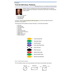
The SMT padstack is easy to define: Top landTop solder maskTop paste maskTop assembly Last week, I explained land calculation for SMT land patterns, so let's discuss plated through-hole calculations in this segment. The through-hole (PTH) padstack is complex. See Figure 1 of a through-hole padstack. Drill holeTop assemblyTop solder maskTop landInner landPlane thermal reliefPlane anti-pad (clearance)Bottom landBottom solder maskBottom assembly Figure 1. The PTH padstack creation can be fully automated via the maximum lead diameter. The CircuitCalculator.com Blog » PCB Trace Width Calculator. This Javascript web calculator calculates the trace width for printed circuit boards based on a curve fit to IPC-2221 (formerly IPC-D-275).

Also see the via calculator. New features: Results update as you type Several choices of units Units and other settings are saved between sessions Blog format allows user comments Inputs: Optional Inputs: Results for Internal Layers: Results for External Layers in Air: Notes: The trace width is calculated as follows: First, the Area is calculated: Area[mils^2] = (Current[Amps]/(k*(Temp_Rise[deg. Then, the Width is calculated: Width[mils] = Area[mils^2]/(Thickness[oz]*1.378[mils/oz])