
Official Site of Pritchard Amps. Tunnel Back™ Cabinets The Tunnel Back™ Speaker System differs from other systems in the way it deals with the natural resonance of the speaker or driver.

Here they are: Tunnel Back™ Cabinet Theory The accompanying drawing is the cross section of the 1-12 cabinet. It shows a front-mounted speaker connected to a speaker board. The column of air lowers the resonant frequency by effectively adding weight to the speaker cone. In addition to lowering the resonant frequency of the speaker, the column of air in the tunnel acts as an acoustic crossover between the front and rear sonic waves. Since the bass is not cancelled the cabinet amazingly sounds bigger than it is. Although this particular concept is used often in the Pritchard Amps combos, there are other variations on this theme more applicable to other speaker forms, such as found in the single 15 extension cabinets.
Ported and Transmission Line Cabinet Problems. FET vs BJT Audio Amplifiers - Blogs - 41hz Forum. Space Charge and Other Low-Voltage Tubes. Huh?
Tubes Running with 12V on the Plates? Yup. That, or even less. You don't have to risk your skin building 250V power supplies just to build a simple radio receiver with tubes. Note well that this applies almost exclusively to receivers. There are two tricks that make this possible: Some tubes have always had the ability to work at low voltages. Let's talk about the tubes designed specifically for 12V operation first. "Space Charge" Tubes for Car Radios Way back in the late 1950s, engineers at Tung-Sol decided to do away with vibrator power supplies in car radios. These tubes worked on something called the "space charge" principle, which basically used the first grid after the cathode to accelerate electrons toward the weakly-charged plate, which was now working at 12V instead of 180-3/Receiving%20Tubes%20Part%202/12DS7-A.PDF">Data PDF) Tech Tips for Space-Charge Tubes The best way to get a sense for space-charge tubes is to study some real circuits.
Cathode Bypass Capacitor Calculator. What does this calculator do?
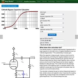
The cathode resistor in a typical triode preamp is bypassed with a large capacitor to eliminate a form of negative feedback known as "cathode degeneration. " This substantially increases gain. When the capacitor is large enough, it acts as a short circuit for audio frequencies, eliminating the negative feedback, but as an open circuit for DC, thereby maintaining DC grid bias. We can introduce treble boost by using a lower capacitor value, one that acts as a short circuit for high frequencies but allows negative feedback to attenuate bass. Design BJT Amplifiers For Given Gain & Impedences. FET Amp Designing. Undefined These pages are meant mainly for engineering students studying in second year( Mumbai university only).
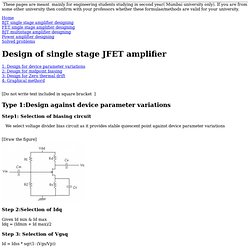
If you are from some other university then confirm with your professors whether these formulae/methods are valid for your university. HomeBJT single stage amplifier designingFET single stage amplifier designingBJT multistage amplifier designingPower amplifier designingSolved problems 1: Design for device parameter variations2: Design for midpoint biasing3: Design for Zero thermal drift4: Graphical methord [Do not write text included in square bracket ] Type 1:Design against device parameter variations Step1: Selection of biasing circuit We select voltage divider bias circuit as it provides stable quiescent point against device parameter variations [Draw the figure] Step 2:Selection of Idq Given Id min & Id max Idq = (Idmin + Id max)/2 Step 3: Selection of Vgsq Id = Idss * sqr(1- (Vgs/Vp)) Vgs = Vp * (1 - sqrt(Id/Idss))
Keith W. Whites EE 320/320L Electronics I. Basic BJT Amplifier Configurations. Common Base Configuration Here the base is the common terminal.
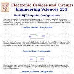
Used frequently for RF applications, this stage has the following properties. Low input impedance, high output impedance, unity (or less) current gain and high voltage gain.Common Collector Configuration. How to design an Amplifier using given Gain, Input Impedance and output Impedance. Lets take this as an example to design a transistor amplifier which achieves these three basic requirements.
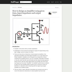
Gain of 50Input impedance of 10kΩOutput impedance of 10Ω.
Design a Depletion-Mode FET Preamp: Curve Method, Part 1. Tube Data. Audio Design Guide. Designing JFET Audio PreAmplifiers. Transconductance The ability of a JFET to amplify is described as trans-conductance and is merely the change in drain current divided by the change in gate voltage.
It is indicated as Mhos or Siemens and is typically 2.5mmhos to 7.5mmhos for the MPF102 transistor. Because of the high input impedance, the gate is considered an open circuit and draws no power from the source. Although voltage gain appears low in a JFET, power gain is almost infinite. Drain Characteristics Even though no voltage appears at the gate, a substantial amount of current will flow from the drain to the source. Minimum Rds(on) or On State Resistance The above value can be determined by reading specification sheets for the selected transistor. MPF102 - 20ma 2N3819 - 22ma 2N4416 - 15ma When designing a JFET circuit, it is highly recommended to prevent the absolute maximum current from being exceeded under any conditions.
JFET Design Example 1 Vcc = 12 Minimum Rds(on) = 0 Ids = 5 ma.