
Addison Engineering
A leading supplier of silicon wafers, wafer processing, semiconductor Equipment, Ceramic Packages, Wafer fabrication, chip carriers and operation Management
Semiconductor wafer - addisonengineering -wollongong-classifieds. <div style="height:30px;border:3px solid #6699ff;text-align:center;font-weight: bold;padding-top:10px"> Your browser does not support JavaScript!

</div> semiconductor wafer - addisonengineering It is most widely distributed in dusts, sands, planetoids, and planets as various forms of silicon dioxide (silica) or silicates. Silicon is the second most abundant element in the Earth's crust.Elemental silicon also has a large impact on the modern world economy. Although most free silicon is used in the steel refining, aluminum-casting, and fine chemical industries, the relatively small portion (< 10%) of very high purity silicon that is used in semiconductor electronics is perhaps the most critical. The use of silicon in semiconductor devices requires a much higher purity than metallurgical grade silicon. Visit our site www.addisonengineering.com/about-silicon.html Contact name : addisonengineering. Semiconductor wafer - addisonengineering-newcastleclassifieds. <div style="height:30px;border:3px solid #6699ff;text-align:center;font-weight: bold;padding-top:10px"> Your browser does not support JavaScript!

</div> semiconductor wafer - addisonengineering It is most widely distributed in dusts, sands, planetoids, and planets as various forms of silicon dioxide (silica) or silicates. Silicon is the second most abundant element in the Earth's crust.Elemental silicon also has a large impact on the modern world economy. Although most free silicon is used in the steel refining, aluminum-casting, and fine chemical industries, the relatively small portion (< 10%) of very high purity silicon that is used in semiconductor electronics is perhaps the most critical. The use of silicon in semiconductor devices requires a much higher purity than metallurgical grade silicon.
Semiconductor wafer - addisonengineering-ads-mall.com. Semiconductor wafer - addisonengineering. Semiconductor wafer - addisonengineering It is most widely distributed in dusts, sands, planetoids, and planets as various forms of silicon dioxide (silica) or silicates.

Silicon is the second most abundant element in the Earth's crust.Elemental silicon also has a large impact on the modern world economy. Although most free silicon is used in the steel refining, aluminum-casting, and fine chemical industries, the relatively small portion (< 10%) of very high purity silicon that is used in semiconductor electronics is perhaps the most critical. The use of silicon in semiconductor devices requires a much higher purity than metallurgical grade silicon. Very pure silicon (>99.9%) can be extracted directly from solid silica or other silicon compounds by molten salt electrolysis.
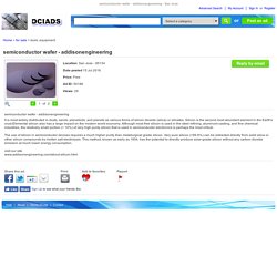
Semiconductor wafer - addisonengineering - DCIADS. Location: San Jose - 95134 Date posted 15 Jul 2016 Price: Free Ad ID: 50186 Views: 29.
Semiconductor wafer - addisonengineering-pluzs.com. Semiconductor wafer - addisonengineering It is most widely distributed in dusts, sands, planetoids, and planets as various forms of silicon dioxide (silica) or silicates.
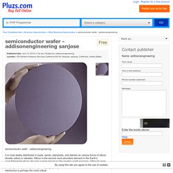
Silicon is the second most abundant element in the Earth's crust.Elemental silicon also has a large impact on the modern world economy. Although most free silicon is used in the steel refining, aluminum-casting, and fine chemical industries, the relatively small portion (< 10%) of very high purity silicon that is used in semiconductor electronics is perhaps the most critical.
The use of silicon in semiconductor devices requires a much higher purity than metallurgical grade silicon. Very pure silicon (>99.9%) can be extracted directly from solid silica or other silicon compounds by molten salt electrolysis. Semiconductor wafer - addisonengineering-adpartisan.net. Semiconductor wafer - addisonengineering It is most widely distributed in dusts, sands, planetoids, and planets as various forms of silicon dioxide (silica) or silicates.

Silicon is the second most abundant element in the Earth's crust.Elemental silicon also has a large impact on the modern world economy. Although most free silicon is used in the steel refining, aluminum-casting, and fine chemical industries, the relatively small portion (< 10%) of very high purity silicon that is used in semiconductor electronics is perhaps the most critical.
The use of silicon in semiconductor devices requires a much higher purity than metallurgical grade silicon. Very pure silicon (>99.9%) can be extracted directly from solid silica or other silicon compounds by molten salt electrolysis. Visit our site www.addisonengineering.com/about-silicon.html. Electronic grade silicon method - addisonengineering -freewebads.biz.
Electronic grade silicon method - addisonengineering - Cathaylist.com. Electronic grade silicon method - Addison Engineering - backpage.com. Electronic grade silicon method - addisonengineering-expatriates.com. Leaded chip carriers - Addison Engineering- HasToGo. Silicon Wafers -zoozads.com. San Diego : Silicon Wafers - Addison Engineering Inc -vendanything.com. Listing Began: July 4, 2016, 12:45 pm Number of Times Viewed: 138 Seller's Comments and Description: Silicon Wafers Addison Engineering stocks over 3-million silicon wafers in diameters of 2", 3", 100mm, 125mm, 150mm, 200mm, 300mm, and 450mm.

We can accommodate small and large quantity requests with diverse specification requirements. Specialty Products Extra Thin WafersSilicon RingsQuartz (fused silica)Pyrex (borosilicate)Soda Lime Czochralski or Float Zone &nbs p; &n bsp; &nbs p; · Prime · Test · Reclaim. Silicon wafers – Addison Engineering-nashikclassifieds.com. Silicon wafers A leading supplier of silicon wafers, wafer processing, semiconductor Equipment, Ceramic Packages, Wafer fabrication, chip carriers and operation Management Addison Engineering stocks over 3-million silicon wafers in diameters of 2″, 3″, 100mm, 125mm, 150mm, 200mm, 300mm, and 450mm.
We can accommodate small and large quantity requests with diverse specification requirements. Our prices are usually lower than test wafer prices from major prime producers. With over 20 years in the semiconductor industry, Addison’s engineers can provide you with the level of support you need Kyocera and NTK manufactured ceramic packages and metal alloy lids. we are suppliers of Side braze, pin grid array, chip carriers, flatpacks, headers, cerdip visit our site When you call, don't forget to mention that you found this ad on nashikclassifieds.com I do not wish to be contacted by telemarketers or representatives of any other website. Silicon wafers – Addison Engineering. Silicon wafers - Addison Engineering-classifieds777.com. Free Classifieds silicon wafers - Addison Engineering. Silicon Wafers-Addison Engineering-The E-waseet Classifieds.
Silicon wafers - Addison Engineering -anyads.co.uk. Silicon wafers A leading supplier of silicon wafers, wafer processing, semiconductor Equipment, Ceramic Packages, Wafer fabrication, chip carriers and operation Management Addison Engineering stocks over 3-million silicon wafers in diameters of 2", 3", 100mm, 125mm, 150mm, 200mm, 300mm, and 450mm.

We can accommodate small and large quantity requests with diverse specification requirements. Our prices are usually lower than test wafer prices from major prime producers. With over 20 years in the semiconductor industry, Addison's engineers can provide you with the level of support you need Kyocera and NTK manufactured ceramic packages and metal alloy lids. we are suppliers of Side braze, pin grid array, chip carriers, flatpacks, headers, cerdip visit our site Share Avoid scams by acting locally or paying with PayPal Never pay with Western Union, Moneygram or other anonymous payment services Don't buy or sell outside of your country. Silicon wafers - Addison Engineering -kyispclassifieds.net.
Silicon wafers A leading supplier of silicon wafers, wafer processing, semiconductor Equipment, Ceramic Packages, Wafer fabrication, chip carriers and operation Management Addison Engineering stocks over 3-million silicon wafers in diameters of 2", 3", 100mm, 125mm, 150mm, 200mm, 300mm, and 450mm.
We can accommodate small and large quantity requests with diverse specification requirements. Our prices are usually lower than test wafer prices from major prime producers. With over 20 years in the semiconductor industry, Addison's engineers can provide you with the level of support you need Kyocera and NTK manufactured ceramic packages and metal alloy lids. we are suppliers of Side braze, pin grid array, chip carriers, flatpacks, headers, cerdip visit our site. Wafer orientation -Addison Engineering-Adpost.com. Trib Classifieds -silicon wafers -Addison Engineering. Leaded chip carriers - Addison Engineering.
Wafer orientation - Addison Engineering. Location: California, California 95134 United States, Ad#: 1345986, Seller: Addisonengineering, Member Since: Jan 28, 2016, Date Posted: Jun 15, 2016, Ad Views: 50 , Company name: addisonengineering, Phone: (408) 926-5000 wafer orientation A leading supplier of silicon wafers, wafer processing, semiconductor Equipment, Ceramic Packages, Wafer fabrication, chip carriers and operation Management Prime Grade Wafers Prime wafers are the highest grade of commercial silicon wafers. They are referred to as device-quality. Test and Monitor Grade Wafers Test or monitor wafers can be used for a variety of purposes, especially in equipment testing and other applications where a large quantity of wafers is necessary (marathon runs). Visit our site www.addisonengineeri ng.com/about-wafers.html Find more listings like wafer orientation - Addison Engineering by searching the Other Business Opportunities category.
Addison Engineering, Inc. - San Jose, CA -Kudzu.com. Home ServicesAutomotiveHealthArticlesRegisterSign In Explore ▼ Home ServicesAutomotiveHealthArticlesWhat It Costs Business Services>Business ConsultingBusiness ServicesBusiness Consulting Addison Engineering, Inc. 0 star rating0 Reviews (408) 926-5000(408) 926-5000www.addisonengineering.com »View Website » Wafer Orientation - Addison Engineering-Salesspider. Wafer orientation A leading supplier of silicon wafers, wafer processing, semiconductor Equipment, Ceramic Packages, Wafer fabrication, chip carriers and operation Management Prime Grade Wafers Prime wafers are the highest grade of commercial silicon wafers.
They are referred to as ? Ceramic Packages - Addison Engineering Inc -cecaca.com. Addison Engineering Incorporated in San Jose. Silicon wafer processing - Addison Engineering -Forstate.com. Multilayer Substrate - Addison Engineering - Claz.org. Leaded chip carriers - Addison Engineering -myadsclassified. Storeboard -Addison Engineering - San Jose - California. Weebly - Addison Engineering Inc. Zipleaf.us -Addison Engineering INC - San Jose, Ca, United States.
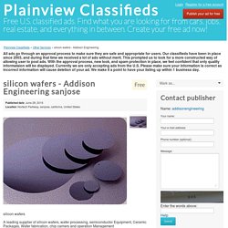
150 Nortech Parkway San Jose, CA 95134, San Jose, Ca, California, 95134, United States About Addison Engineering INC Established April 2000 Addison Engineering, Inc., founded in 1983, is a leading supplier of silicon wafers, silicon wafer processing, semiconductor process, test, and assembly equipment, silicon wafer operations management, ceramic packages and related semiconductor materials and services. Our success can be credited to our consistent high quality service and our immediate response to our customers' needs. Our customers value us because they know we are selective about the commitments we take on, and we are serious about meeting them. For more info, please visit : Photo Gallery Location Use two fingers to move the map. Diigo -Addisonengineering Inc. Delicious -Addison Engineering Inc. Showmelocal.com-Addison Engineering Inc - San Jose, CA 95134 - (408)926-5000. Solar Wafers -epage -Addison Engineering Inc.
Addison Engineering Inc in San Jose, CA 95134. Addison Engineering, Inc. Equipment Division Home. Addison Engineering Inc. Behance - Addison Engineering Inc. Addison Engineering Inc - Alviso, San Jose, California 95134 (7486767) Bundlr - Addison Engineering Inc. Scoop.it-Addison Engineering Inc. Google Plus -Addison Engineering Inc. Facebook -Addison Engineering, Inc. Addison Engineering Inc - San Jose, CA 95134 - (408)926-5000-showmelocal.com. Pinterest -Addison Engineering Inc. Discover and save creative ideas There’s more to see... Come take a look at what else is here!
He used Pinterest to dive deep Join Pinterest to find (and save!) All the things that inspire you. Oops! Or Back Customize my signup experience using info from sites I’ve visited.Learn more Continue as a business Creating an account means you’re okay with Pinterest's Terms of Service, Privacy Policy billion Pins to explore seconds to sign up (free!) About Pinterest Blog Businesses Terms & Privacy Help iPhone App Android App Discover Pinterest: Gardening Travel Kids Weddings Humor Quotes DIY Design Animals Sitemap International.
Crunchbase -Addison Engineering Inc. Addison Engineering Inc -Tumblr. Ceramic packages - Addison Engineering. Addisonengineering - Silicon Wafer Processing. Waferprocessing -Addison Engineering. Wafer formation -Addison Engineering. Monocrystalline silicon - Addison Engineering. Chipcarriers -Addison Engineeirng. Silicon wafers - Addison Engineering. Ceramic Packages - Addison Engineering Inc. Silicon Wafer Processing- Addison Engineering Inc. Addison Engineering's Likes -Stumbleupon. Silicon wafers - addisonengineering.com. Contact Addison - A leading supplier of silicon wafers. Solar Cell Wafers: Addison Engineering. Solar Cell Wafers Materials Various materials display varying efficiencies and have varying costs. Materials for efficient solar cells must have characteristics matched to the spectrum of available light. Some cells are designed to efficiently convert wavelengths of solar light that reach the Earth surface.
However, some solar cells are optimized for light absorption beyond Earth's atmosphere as well. Light absorbing materials can often be used in multiple physical configurations to take advantage of different light absorption and charge separation mechanisms. Materials presently used for photovoltaic solar cells include monocrystalline silicon, polycrystalline silicon, amorphous silicon, cadmium telluride, and copper indium selenide/sulfide. Many currently available solar cells are made from bulk materials that are cut into wafers between 180 to 240 micrometers thick that are then processed like other semiconductors.
Manufacture. MEMS: Addison Engineering. MEMS (Microelectromechanical Systems) Semiconductors: Addison Engineering. A semiconductor device, is an electronic circuit component made from a material that is neither a good conductor nor a good insulator (hence semiconductor). Such devices have found wide applications because of their compactness, reliability, and low cost. About Wafers: Interesting information about silicon wafers. In electronics, a wafer (also called a slice or substrate) is a thin slice of semiconductor material, such as a silicon crystal, used in the fabrication of integrated circuits and other microdevices. The wafer serves as the substrate for microelectronic devices built in and over the wafer and undergoes many microfabrication process steps such as doping or ion implantation, etching, deposition of various materials, and photolithographic patterning.
Silicon Facts: Electronics grade silicon and silicon wafers. About Silicon Silicon is a chemical element with the symbol Si and atomic number 14. Semiconductor equipment manufacturing Process -Addison Engineering. Silicon wafer fabrication processing- Addison Engineering. Ceramic IC Packages and Multilayer Substrate - Addison Engineering. Silicon wafers producers and suppliers company - Addison Engineering. Silicon wafers,wafer processing,ceramic packages,semiconductor Equipment-Addison Engineering.